


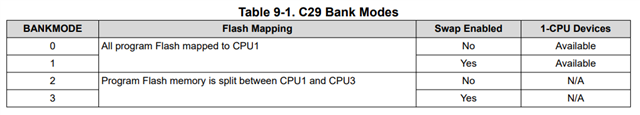
I actually have it working now with this process. I changed the cmd files for both CPUS to have all flash address for CPU3 starting 0x103xxxxx. I tried the process above with that and it failed to write the 0x1030000 flash space for CPU 3 in step 4. Change back to original and now blinky works and even an adaptation for our own dual core works too. Really curious to what might have happened here? Also been looking for a memory map which details the default mapping for the SRAM/FLASH but cannot find anything. Does something exist?
Almost like some issue with the board that needed writing or resetting?

 (snippet of Memory Map section in datasheet)