


Part Number: TMS320F28P650DK
Recently, I have been developing the bootloader for the F28P65. Currently, all functions have been basically completed. The BANK0 of FLASH stores the BL program, and in the debugging configuration, it is set to only erase BANK0. The BANK2 of FLASH stores the APP program, and in the debugging configuration, it is set to only erase BANK2.
When I used CCS to download the APP program to BANK2, FLASH BANK2 failed to erase and the following prompt appeared:
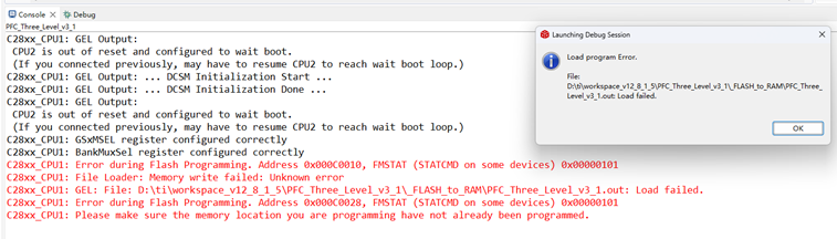
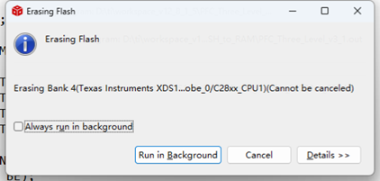
Even if I choose to erase all the FLASH when downloading the APP program to BANK2 using CCS, only BANK0, BANK1 and BANK4 will display the erase dialog box, as shown in the following figure:
If I use the FLASH API in the bootloder program to erase BANK2, the erasure will be successful. Then, when I download the APP program to BANK2 using CCS, the programming will also be successful. What I find most confusing is why CCS doesn't erase the correct BANK before downloading the program?
thank you~~
