Part Number: C2000WARE
Other Parts Discussed in Thread: LAUNCHXL-F28P65X, , SYSCONFIG
CCS Version: 20.2.0.12__1.8.0
C2000Ware Version: C2000Ware_6_00_01_00
Description of the Issue: I am working with the dual-core LED blink example on the LAUNCHXL-F28P65X.
-
When I comment out the CPU2 boot-related code in the CPU1 project and flash only CPU1, the LED blinks as expected.
-
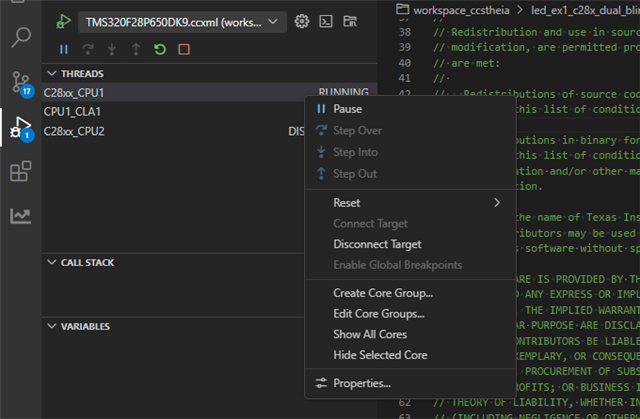
However, when I include the CPU2 boot code in CPU1 and attempt to load/write the CPU2 project to the device, I encounter the following error:
C28xx_CPU1: If erase/program (E/P) operation is being done on one core, the other core should not execute from shared-RAM (SR) as they are used for the E/P code. User code execution from SR could commence after the selected flash banks are programmed.
C28xx_CPU1: Only CPU1 on-chip Flash Plugin can configure clock for CPU1, and CPU2 Flash operations. Plugin automatically configures PLL when CPU1 Flash operations are invoked. However, if users want to do only CPU2 Flash operations without doing a prior CPU1 operation in the current session, they should click on 'Configure Clock' button in CPU1's on-chip Flash Plugin before invoking CPU2 Flash operations. When this button is used, Flash Plugin will configure the clock for CPU1/CPU2 at 200MHz using INTOSC as the clock source. Plugin will leave PLL config like this and user application should configure the PLL as required by application.
C28xx_CPU1: Before doing any flash operations using the flash plugin, (a) Please select which flash banks should be mapped to which CPU (CPU1 vs CPU2) - This selection should be done in CPU1 flash plugin GUI. (b) Please select the flash banks that the user would like the flash plugin to erase (in the CPU1 flash plugin GUI and the CPU2 flash plugin GUI)
C28xx_CPU2: If erase/program (E/P) operation is being done on one core, the other core should not execute from shared-RAM (SR) as they are used for the E/P code. User code execution from SR could commence after the selected flash banks are programmed.
C28xx_CPU2: Only CPU1 on-chip Flash Plugin can configure clock for CPU1, and CPU2 Flash operations. Plugin automatically configures PLL when CPU1 Flash operations are invoked. However, if users want to do only CPU2 Flash operations without doing a prior CPU1 operation in the current session, they should click on 'Configure Clock' button in CPU1's on-chip Flash Plugin before invoking CPU2 Flash operations. When this button is used, Flash Plugin will configure the clock for CPU1/CPU2 at 200MHz using INTOSC as the clock source. Plugin will leave PLL config like this and user application should configure the PLL as required by application.
C28xx_CPU2: Before doing any flash operations using the flash plugin, (a) Please select which flash banks should be mapped to which CPU (CPU1 vs CPU2) - This selection should be done in CPU1 flash plugin GUI. (b) Please select the flash banks that the user would like the flash plugin to erase (in the CPU1 flash plugin GUI and the CPU2 flash plugin GUI)
C28xx_CPU2: GSxMSEL register configured correctly
C28xx_CPU2: Flash Programmer: Error erasing Bank 0 FMSTAT (STATCMD on some devices) value = 65 (decimal). Operation Cancelled (0).
C28xx_CPU2: File Loader: Memory write failed: Unknown error
C28xx_CPU2: GEL: File: C:\Users\PNE\workspace_ccstheia\led_ex2_blinky_sysconfig_cpu2\FLASH\led_ex2_blinky_sysconfig_cpu2.out: Load failed.
My Modifications:
-
Added
_LAUNCHXL_F28P65Xto the Predefined Symbols in the C2000 Compiler options for both CPU1 and CPU2 projects.
Questions:
-
Are there additional symbols or build configurations required for the F28P65X launchpad specifically for dual-core operation?
-
Does the linker command file (.cmd) for the example need specific modifications to avoid memory conflicts during the CPU2 flash process?
-
Is there a specific sequence I should follow when connecting and loading the two cores in CCS?