Because of the holidays, TI E2E™ design support forum responses will be delayed from Dec. 25 through Jan. 2. Thank you for your patience.

This thread has been locked.

If you have a related question, please click the "Ask a related question" button in the top right corner. The newly created question will be automatically linked to this question.

TMS320F2812 PROBLEM GPIO PORT B

Other Parts Discussed in Thread: TMS320F2812

Hi, 

     am using my custom  tms320f2812 kit for solar project., am providing inverter pulse using tms320f2812 EVB from the PORTB0 - PORTB3 to IGBT driver board , at reset state or initial stage all these pins high ., 

How should i avoid this high on port lines ? if all inverter pins are high then all the IGBT devices are turn on condition. , so the VDC + and - will short in power circuit/solar input .

  • Hi Thiyagu,

    How should i avoid this high on port lines ?

    Just check whether you've disabled the internal pull-up? Generally its GPxPUD register.

    Regards,

    Gautam

  • Gautam, 

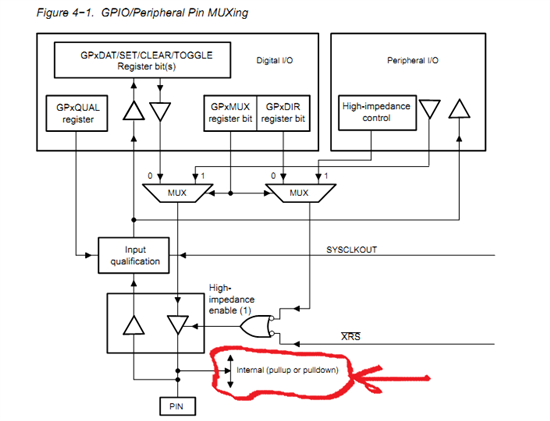
         I checked fully it doesnt have any GPxPUD register., 

  • Thiyagarajan . S said:

    Gautam, 

         I checked fully it doesnt have any GPxPUD register., 

    So did you check the GPIO internal diagram? Are they all internally pulled up? If so then check which register is linked with this feature.

    Regards,

    Gautam

  • Gautam,

                 yeah, their is no internal pull up or pull down enable register. i attached the gpio functional diagram kindly check it . i wanna to pull down the Portb0 to portb7 for my project initially. i drive pwm pulse with these pins. 

  • You would like to check these threads:

    http://e2e.ti.com/support/microcontrollers/c2000/f/171/t/85331.aspx

    http://e2e.ti.com/support/microcontrollers/c2000/f/171/t/107175.aspx

    Actually, the latest ones have GPxPUD register and hence no issues here. F2812 doesn't seem to have such kind of a feature.

    Regards,

    Gautam

  • Thiyagu,


    Could you share your Event Manager and GPIO configuration for PWM?

    Regards,

    Richard

  • Gautam,

           I checked the link which you send in previous post.

    At this link :  http://e2e.ti.com/support/microcontrollers/c2000/f/171/t/107175.aspx

      said : On the F281x devices TI requires the VDDIO rail to be powered before VDD. This is to ensure a proper reset inside of the device during power up, particularly with respect to the flash. Unfortunately, powering up VDDIO first on these devices allows the output buffers to drive (usually low, but possibly high) during the power up procedure. Once the device is fully powered and the device receives its first clock pulse the output buffer will be turned off. However, there are weak internal pullup circuits on these pins, so they should weakly drive high until code starts and configures them. On later devices TI created a power sequence to keep  the I/Os from glitching, eventually removing all power sequencing on the latest devices. They also removed the pullups on PWM pins on later devices. However for the F281x series you have to protect your predrivers externally during powerup.


    I highlighted one line in the above paragraph.,  i captured the VDDIO and VDD PIN POWER UP STATE .,  and i attached ., kindly check and tell .... 

    My issues is : after the program being flashed in F2812, the PWM pins are high when power-on reset after executing  the code the pwm pins are outting the pwm pulses good., .  

    Example : after flash the code, i power off. and if i again  power up the TMS320F2812, upto to 100ms all the pins high later it producing pulses..  i want to avoid that high , because my three phase igbt driver will spoill if all the six pwm pulses are high at a time.  i want to solve this issues 


    Many Thanks

    Thiyagarajan . S