Hello everyone,
I am using the 28335 delfino and struggle to get the Digital Controller Library running. I consulted the user guide (SPRUI31) which on page 15 and 16 describes how to add the DCL to my code.
In particular, step #3 on page 16 gives me headache as I have no real experience with the linker command file as for now (and consequently struggle to find the proper information in the SPRU513 documentation). In particular, step #3 says:
"...C28x library functions are placed in the user-defined code section “dclfuncs”. An example showing how this section might be mapped into the internal L4 RAM memory block is shown below:
dclfuncs : > RAML4, PAGE = 0
..."
When I look at the 28335_RAM_Ink.cmd linker command file, there is no such thing as dclfuncs. The same applies to the DSP2833x_Headers_nonBIOS.cmd linker command file.
I would appreciate it if you could guide me in this matter.
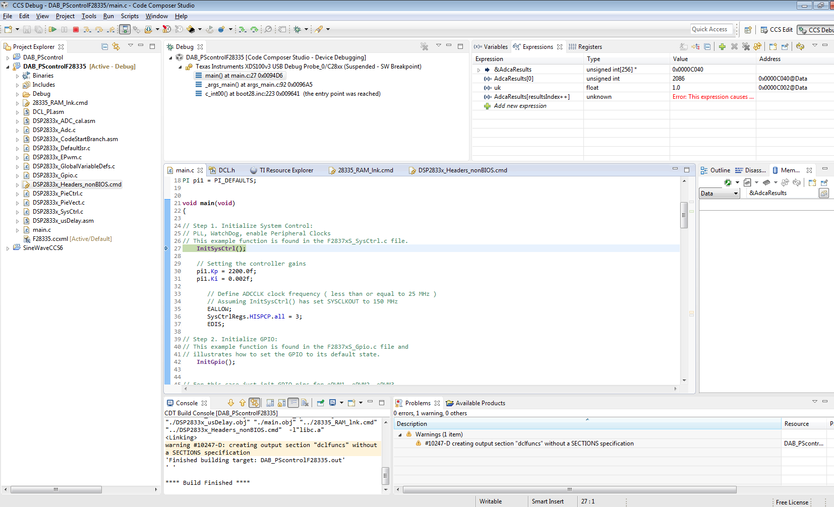
Please find a screenshot of where I currently am, as well as the C code of my current project.
#include "DSP28x_Project.h"     // Device Headerfile and Examples Include File
#include <math.h>
#include "DCL.h"				// Header file for digital control purposes

// Prototype statements for functions found within this file.
void InitEPwm2(void);
void InitializeADC(void);

__interrupt void adc_isr(void);

// User defined
double PRD;
#define RESULTS_BUFFER_SIZE 256 //buffer for storing conversion results
Uint16 AdcaResults[RESULTS_BUFFER_SIZE];
Uint16 resultsIndex;
volatile Uint16 bufferFull;
float uk;	// control
PI pi1 = PI_DEFAULTS;


void main(void)
{

// Step 1. Initialize System Control:
// PLL, WatchDog, enable Peripheral Clocks
// This example function is found in the F2837xS_SysCtrl.c file.
    InitSysCtrl();

	// Setting the controller gains
	pi1.Kp = 2200.0f;
	pi1.Ki = 0.002f;

	   // Define ADCCLK clock frequency ( less than or equal to 25 MHz )
	   // Assuming InitSysCtrl() has set SYSCLKOUT to 150 MHz
	   EALLOW;
	   SysCtrlRegs.HISPCP.all = 3;
	   EDIS;

// Step 2. Initialize GPIO:
// This example function is found in the F2837xS_Gpio.c file and
// illustrates how to set the GPIO to its default state.
    InitGpio();


// For this case just init GPIO pins for ePWM1, ePWM2, ePWM3
// These functions are in the F2837xS_EPwm.c file
	InitEPwm2Gpio();
	InitAdc();  // For this example, init the ADC

// Step 3. Clear all interrupts and initialize PIE vector table:
// Disable CPU interrupts
    DINT;

// Initialize the PIE control registers to their default state.
// The default state is all PIE interrupts disabled and flags
// are cleared.
// This function is found in the F2837xS_PieCtrl.c file.
    InitPieCtrl();

// Disable CPU interrupts and clear all CPU interrupt flags:
    IER = 0x0000;
    IFR = 0x0000;

// Initialize the PIE vector table with pointers to the shell Interrupt
// Service Routines (ISR).
// This will populate the entire table, even if the interrupt
// is not used in this example.  This is useful for debug purposes.
// The shell ISR routines are found in F2837xS_DefaultIsr.c.
// This function is found in F2837xS_PieVect.c.
    InitPieVectTable();

// Interrupts that are used in this example are re-mapped to
// ISR functions found within this file.
	EALLOW; // This is needed to write to EALLOW protected registers
//	PieVectTable.EPWM2_INT = &epwm2_isr;	//function for ePWM2 interrupt
	PieVectTable.ADCINT = &adc_isr;
	EDIS;   // This is needed to disable write to EALLOW protected registers

// Step 4. Initialize the Device Peripherals:
// For this example, only initialize the ePWM and ADC

	EALLOW;
	SysCtrlRegs.PCLKCR0.bit.TBCLKSYNC = 0;
	EDIS;

	InitEPwm2();
	InitializeADC();


    //Initialize results buffer
        for(resultsIndex = 0; resultsIndex < RESULTS_BUFFER_SIZE; resultsIndex++)
        {
        	AdcaResults[resultsIndex] = 0;
        }
        resultsIndex = 0;
        bufferFull = 0;

	EALLOW;
	SysCtrlRegs.PCLKCR0.bit.TBCLKSYNC =1;
	EDIS;

	// Enable ADCINT in PIE
	   PieCtrlRegs.PIEIER1.bit.INTx6 = 1;
	   IER |= M_INT1; // Enable CPU Interrupt 1
	   EINT;          // Enable Global interrupt INTM
	   ERTM;          // Enable Global realtime interrupt DBGM
// Step 6. IDLE loop. Just sit and loop forever (optional):
    //take conversions indefinitely in loop
        do
        {
        	//wait while ePWM causes ADC conversions, which then cause interrupts,
        	//which fill the results buffer, eventually setting the bufferFull
        	//flag
        	while(!bufferFull);
        	bufferFull = 0; //clear the buffer full flag
        }while(1);
}

/* Interrupt service routine reading the output voltage and generating the PWM */
__interrupt void adc_isr(void)
{
	AdcaResults[resultsIndex++] = AdcRegs.ADCRESULT0 >>4;
	if(RESULTS_BUFFER_SIZE <= resultsIndex)
	{
		resultsIndex = 0;
		bufferFull = 1;
	}

		uk = DCL_runPI(&pi1, 0xC28, AdcaResults[resultsIndex++]);

			// Generates the new duty cycle
		EPwm2Regs.CMPA.half.CMPA=uk;


		  // Reinitialize for next ADC sequence
		AdcRegs.ADCTRL2.bit.RST_SEQ1 = 1;         // Reset SEQ1
		AdcRegs.ADCST.bit.INT_SEQ1_CLR = 1;       // Clear INT SEQ1 bit
		PieCtrlRegs.PIEACK.all = PIEACK_GROUP1;   // Acknowledge interrupt to PIE
}

void InitEPwm2()
{
    EPwm2Regs.TBPRD = PRD;                       // Set timer period
    EPwm2Regs.TBPHS.half.TBPHS = 0x0000;           // Phase is 0
    EPwm2Regs.TBCTR = 0x0000;                     // Clear counter

    // Setup TBCLK
    EPwm2Regs.ETSEL.bit.SOCAEN = 1;  			//enable SOCA
	EPwm2Regs.ETSEL.bit.SOCASEL	= 4;	        // Select SOC on up-count
	EPwm2Regs.ETPS.bit.SOCAPRD = 1;		        // Generate pulse on 1st event
    EPwm2Regs.TBCTL.bit.CTRMODE = TB_COUNT_UPDOWN; // Count up
    EPwm2Regs.TBCTL.bit.PHSEN = TB_ENABLE;        // Disable phase loading
    EPwm2Regs.TBCTL.bit.PRDLD = TB_SHADOW;
    EPwm2Regs.TBCTL.bit.SYNCOSEL = TB_SYNC_IN;
    EPwm2Regs.CMPCTL.bit.SHDWAMODE = CC_SHADOW;
    EPwm2Regs.CMPCTL.bit.SHDWBMODE = CC_SHADOW;
    EPwm2Regs.CMPCTL.bit.LOADAMODE = CC_CTR_ZERO;
    EPwm2Regs.CMPCTL.bit.LOADBMODE = CC_CTR_ZERO;

    EPwm2Regs.TBCTL.bit.HSPCLKDIV = TB_DIV1;       // Clock ratio to SYSCLKOUT
    EPwm2Regs.TBCTL.bit.CLKDIV = TB_DIV1;          // Slow just to observe on the
                                                   // scope

    // Set actions
    EPwm2Regs.AQCTLA.bit.CAU = AQ_CLEAR;            // Set PWM2A on Zero
    EPwm2Regs.AQCTLA.bit.CAD = AQ_SET;

    EPwm2Regs.AQCTLB.bit.CAU = AQ_SET;          // Set PWM2A on Zero
    EPwm2Regs.AQCTLB.bit.CAD = AQ_CLEAR;

    // Active Low complementary PWMs - setup the deadband
    EPwm2Regs.DBCTL.bit.OUT_MODE = DB_FULL_ENABLE;
    EPwm2Regs.DBCTL.bit.POLSEL = DB_ACTV_HIC;
//    EPwm2Regs.DBCTL.bit.IN_MODE = DBA_ALL;
    EPwm2Regs.DBRED = 100;
    EPwm2Regs.DBFED = 100;

    // Interrupt where we will modify the deadband
    EPwm2Regs.ETSEL.bit.INTSEL = ET_CTR_ZERO;     // Select INT on Zero event
    EPwm2Regs.ETSEL.bit.INTEN = 1;                // Enable INT
    EPwm2Regs.ETPS.bit.INTPRD = ET_1ST;           // Generate INT on 1st event

}
void InitializeADC()
{
	// Configure ADC
	   AdcRegs.ADCMAXCONV.all = 0x0001;       // Setup 2 conv's on SEQ1
	   AdcRegs.ADCCHSELSEQ1.bit.CONV00 = 0x0; // Setup ADCINA3 as 1st SEQ1 conv.
	   AdcRegs.ADCCHSELSEQ1.bit.CONV01 = 0x2; // Setup ADCINA2 as 2nd SEQ1 conv.
	   AdcRegs.ADCTRL2.bit.EPWM_SOCA_SEQ1 = 1;// Enable SOCA from ePWM to start SEQ1
	   AdcRegs.ADCTRL2.bit.INT_ENA_SEQ1 = 1;  // Enable SEQ1 interrupt (every EOS)
}