This thread has been locked.

If you have a related question, please click the "Ask a related question" button in the top right corner. The newly created question will be automatically linked to this question.

CCS/CCSTUDIO: CLA Getting started with C Compiler => CCS V.6/LAUNCHXL-F28377S

Part Number: CCSTUDIO
Other Parts Discussed in Thread: TMS320F28377S, CONTROLSUITE

Tool/software: Code Composer Studio

Hello folks,


i´m about to use the CLA on the TMS320F28377S which is mounted on the launchpad. I´m running CCS V.6
The point is, i can´t really figure out how to use the CLA. My goal is to write C Code for the CLA.

1.) There is a C-Compiler for the CLA which belongs to the the Code generation tools?

2.) Where do i write the Code which is supposed to be loaded into the CLA?
2.1.) From what i understood is, that CLA code is loaded together with the CPU code to the FLASH and then copied into the the RAM of the CLA?
2.2.) Do i write CLA code in the same source files from the CPU? If so, how does the envoironment know, which code has to be compiled for CPU and which for CLA?  Since i read about .cla files, i think C Code for CLA is found in it´s own files? How would a "C source .cla file look like? Can i access Peripheral registers following the "register access approach" like "adcRes = AdcaResultRegs.ADCRESULT0;"

3.) Where do the references of "extern uint32_t Cla1funcsRunStart, Cla1funcsLoadStart, Cla1funcsLoadSize;" come from? Are they user defined or allready existing in library headers? What are thier exact purpose ( i can imagine they deal around to map the CLA code).

best regards,
Jasson

  • Ok,

    i could figure out some things by my own.
    I have defined a .cla file which is recognized by CCS. I know it, because, i get errors within that file ;>
    I have found a .cla file in
    "ti\controlSUITE\device_support\F2837xS\v210\F2837xS_examples_Cpu1\cla_asin\cpu01"

    I have read in the Ti Wiki, it is possible to access GPIO´s from the CLA on my TMS320F28377S. On that i found this thread:

    Toggling a GPIO on CLA - C2000 microcontrollers forum - C2000™︎ microcontrollers - TI E2E support fo...

    e2e.ti.com
    Other Parts Discussed in Thread: TMS320F28377D , TMS320F28075 I am using TMS320F28377D and i found on TI wiki for CLA that On the 2837xD/S, the CLA can directly

    But i´m not sure how to access the CLA´s GPIO registers. For example, do i have to include a file like the "F2837xS_GlobalVariableDefs.c" ?

    best regards!

  • Hi,

    A good place to start are the examples. I would suggest taking one of the existing examples and modifying the contents of the task to suit your purpose. Additionally, you will find tutorials on the CLA C compiler here

    training.ti.com/search-catalog
  • I made it to a point, where i can complie without an error. I have a warning
    "warning #10247-D: creating output section "Cla1Prog" without a SECTIONS  specification"
    Found in another thread (

    HRPWM with Sysbios - C2000 microcontrollers forum - C2000™︎ microcontrollers - TI E2E support forums

    e2e.ti.com
    Other Parts Discussed in Thread: SYSBIOS , TMS320F28069 Hello, I am running into problems, when trying to adapt PWM frequency with HRPWM within my Sysbios application
    )i have to add

    Under the MEMORY section, page 1 add

    1
    2
    CLA1_MSGRAMLOW       : origin = 0x001480, length = 0x000080
    CLA1_MSGRAMHIGH      : origin = 0x001500, length = 0x000080

    Under the SECTIONS, add

    1
    2
    3
    4
    5
    6
    7
    8
    9
    10
    Cla1Prog :  LOAD = FLASHH,
                RUN=RAML3,
                LOAD_START(_Cla1funcsLoadStart),
                LOAD_END(_Cla1funcsLoadEnd),
                LOAD_SIZE(_Cla1funcsLoadSize),
                RUN_START(_Cla1funcsRunStart),
                PAGE = 0
    Cla1ToCpuMsgRAM  : > CLA1_MSGRAMLOW,   PAGE = 1
    CpuToCla1MsgRAM  : > CLA1_MSGRAMHIGH,  PAGE = 1

    There are values, i don´t understand, where they come from, since i´d probably have to adjust them to my TMS320F28377S device
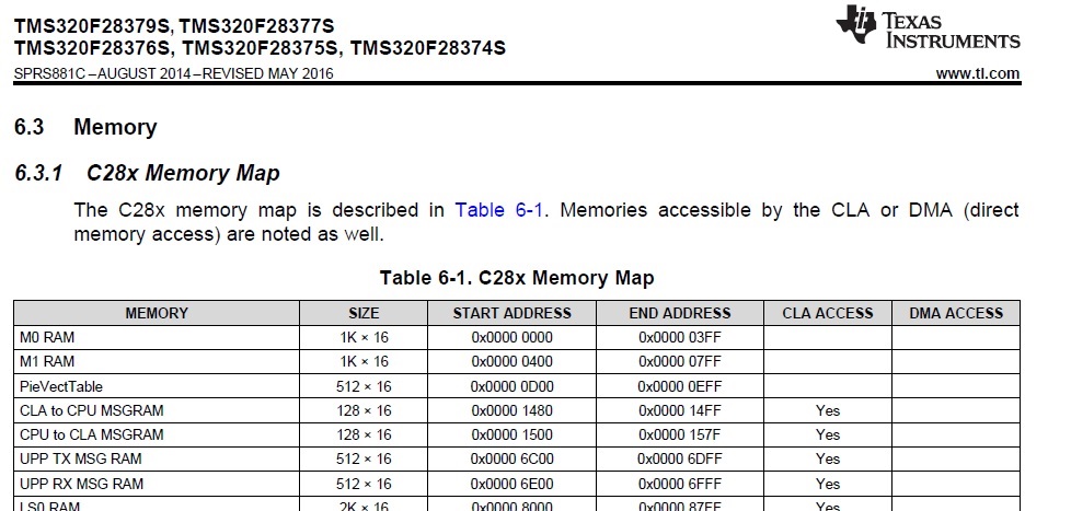
    1.) Where do the origin/length values for the MSGRAMLOW and MSGRAMHIGH  come from?
    2.) Related to the thread i linked, i read there about "the" linker file. Does there exist something like "the" linker file or is it more boundle of severa as i find them in "C:\ti\controlSUITE\device_support\F2837xS\v210\F2837xS_common\cmd"?
    3.) Since i made my start based on "loadable" project examples from the controlSuite, they are configured to run from CPU´s Ram, not FLASH. So i´m not sure about the impact, since the code for the CLA gets "memcopy"´ed from FLASH=>RAM. Do i have to change the CCS configuration from CPU1_RAM to CPU1_FLASH?

  • The origin of your CPU/CLA message ram location can be found in the memory map of the 28377S datasheet.  The memory location is the same on the 28377D.  I've attached the related section.

  • user4221161 said:
    1.) Where do the origin/length values for the MSGRAMLOW and MSGRAMHIGH  come from?

    see Ryan's answer

    user4221161 said:
    2.) Related to the thread i linked, i read there about "the" linker file. Does there exist something like "the" linker file or is it more boundle of severa as i find them in "C:\ti\controlSUITE\device_support\F2837xS\v210\F2837xS_common\cmd"?

    There are several in that folder that you get to choose from. For CLA related projects there are 2, 1 for when you want to run out of RAM (JTAG is always connected) and another for standalone mode (boot to FLASH). When testing you can use the RAM linker file as its quicker to load code to RAM but for release code you will have to switch to the FLASH linker command file

    user4221161 said:
    3.) Since i made my start based on "loadable" project examples from the controlSuite, they are configured to run from CPU´s Ram, not FLASH. So i´m not sure about the impact, since the code for the CLA gets "memcopy"´ed from FLASH=>RAM. Do i have to change the CCS configuration from CPU1_RAM to CPU1_FLASH?

    the CPU1_RAM config allows you to do some quick prototyping and debug of the CLA code itself; its quicker to load up the RAM. For release, use the CPU1_FLASH, you will notice it takes a lot longer to load up. When you do switch over to the FLASH config you will notice the project uses a different linker command file and there is additional code to memcpy CLA code (Cla1Prog)- the CLA can only execute from RAM - and constants (.cla_const) from flash to RAM.

  • Hello and a good new year!


    Allthough i´m not at the finish line, i think i do progess. I have doubt that the CLA Task runs.
    I should have been more percise at the beginning. I have a LAUNCHXL-F28377S and i use the onboard emulator to programm/debug.

    My first goal is simply to switch on a Pin in the CLA´s Task 7, by using the SoftwareForceTask Option. From what i read in the Wiki on TMS320F28377S devices it is possible to access GPIO´s.
    I try to strip down the taken steps to a minimum to achieve that. My project runs in RAM config - so no FLASH is used.

    I want to use RAMLS4 as the program ram for the CLA.

    In the following one finds my code in the pattern
    CLA Memory Config                                               
        (no Message Ram init, since there are no messages used between CPU1 and CLA1)
    Init CLA Task Vectors
    Linker CMD FIle                                                           ( not sure, if i need a scratch Pad area)
    CLA.c File                                                                      (how do i invoke FS2837xS_Gpio.c properly to avoid the "implicid declaration warning?)
    Software Force Task 7 before infinite main loop


    ______________________________________CLA Memory Config Start___________________________________________________________

    void CLA_configClaMemory(void)
    {
        extern uint32_t Cla1funcsRunStart, Cla1funcsLoadStart, Cla1funcsLoadSize;
        EALLOW;
    
    #ifdef _FLASH
        //
        // Copy over code from FLASH to RAM
        //
        memcpy((uint32_t *)&Cla1funcsRunStart, (uint32_t *)&Cla1funcsLoadStart,
               (uint32_t)&Cla1funcsLoadSize);
    #endif //_FLASH
    
        //
        // Initialize and wait for CLA1ToCPUMsgRAM
        //
    //MemCfgRegs.MSGxINIT.bit.INIT_CLA1TOCPU = 1;                                         No messages are going to be used, so no MSG space init
    //while(MemCfgRegs.MSGxINITDONE.bit.INITDONE_CLA1TOCPU != 1){};  No messages are going to be used, so no MSG space init
    
        //
        // Initialize and wait for CPUToCLA1MsgRAM
        //
    //MemCfgRegs.MSGxINIT.bit.INIT_CPUTOCLA1 = 1;                    No messages are going to be used, so no MSG space init
    //while(MemCfgRegs.MSGxINITDONE.bit.INITDONE_CPUTOCLA1 != 1){};  No messages are going to be used, so no MSG space init
    
        //
        // Select LS3RAM to be the programming space for the CLA
        // First configure the CLA to be the master for LS3 and then
        // set the space to be a program block
        //
        MemCfgRegs.LSxMSEL.bit.MSEL_LS3 = 1;
        MemCfgRegs.LSxCLAPGM.bit.CLAPGM_LS3 = 1;
    
        //
        // Next configure LS0RAM and LS4RAM as data spaces for the CLA
        // First configure the CLA to be the master for LS0(1) and then
        // set the spaces to be code blocks
        //
        MemCfgRegs.LSxMSEL.bit.MSEL_LS4 = 1;               // define some space for variables inside GPIO_WritePin()
        MemCfgRegs.LSxCLAPGM.bit.CLAPGM_LS4 = 0;          // define some space for variables inside GPIO_WritePin()
    
    
        EDIS;
    }

    ______________________________________CLA Memory Config END___________________________________________________________


    ______________________________________Init CLA Task Vectors Begin___________________________________________________________
    void CLA_initCpu1Cla1(void)
    {
        //
        // Compute all CLA task vectors
        // On Type-1 CLAs the MVECT registers accept full 16-bit task addresses as
        // opposed to offsets used on older Type-0 CLAs
        //
        EALLOW;
        Cla1Regs.MVECT1 = (uint16_t)(&Cla1Task1);
        Cla1Regs.MVECT2 = (uint16_t)(&Cla1Task2);
        Cla1Regs.MVECT3 = (uint16_t)(&Cla1Task3);
        Cla1Regs.MVECT4 = (uint16_t)(&Cla1Task4);
        Cla1Regs.MVECT5 = (uint16_t)(&Cla1Task5);
        Cla1Regs.MVECT6 = (uint16_t)(&Cla1Task6);
        Cla1Regs.MVECT7 = (uint16_t)(&Cla1Task7);
        Cla1Regs.MVECT8 = (uint16_t)(&Cla1Task8);

        //
        // Enable the IACK instruction to start a task on CLA in software
        // for all  8 CLA tasks. Also, globally enable all 8 tasks (or a
        // subset of tasks) by writing to their respective bits in the
        // MIER register
        //
        Cla1Regs.MCTL.bit.IACKE = 1;
        Cla1Regs.MIER.all = (M_INT8 | M_INT7);
        Cla1SoftIntRegs.SOFTINTEN.bit.TASK7 = 1;   //Enable Software Trigger for Task 7

        //
        // Configure the vectors for the end-of-task interrupt for all
        // 8 tasks
        //
        PieVectTable.CLA1_1_INT = &cla1Isr1;
        PieVectTable.CLA1_2_INT = &cla1Isr2;
        PieVectTable.CLA1_3_INT = &cla1Isr3;
        PieVectTable.CLA1_4_INT = &cla1Isr4;
        PieVectTable.CLA1_5_INT = &cla1Isr5;
        PieVectTable.CLA1_6_INT = &cla1Isr6;
        PieVectTable.CLA1_7_INT = &cla1Isr7;
        PieVectTable.CLA1_8_INT = &cla1Isr8;


        //
        DmaClaSrcSelRegs.CLA1TASKSRCSEL2.bit.TASK7 = 0; //SW Trigger

        //
        // Enable CLA interrupts at the group and subgroup levels
        //
        //PieCtrlRegs.PIEIER11.all = 0xFFFF;
        //IER |= (M_INT11 );
        EDIS;
    }
    ______________________________________Init CLA Task Vectors End___________________________________________________________

    ______________________________________Linker CMD FIle Begin___________________________________________________________

    MEMORY
    {
    PAGE 0 :
       /* BEGIN is used for the "boot to SARAM" bootloader mode   */

       BEGIN               : origin = 0x000000, length = 0x000002
       RAMM0               : origin = 0x000122, length = 0x0002DE
       RAMD0               : origin = 0x00B000, length = 0x000800
       RAMLS0              : origin = 0x008000, length = 0x000800
       RAMLS1              : origin = 0x008800, length = 0x000800
       RAMLS2              : origin = 0x009000, length = 0x000800
       RAMLS3              : origin = 0x009800, length = 0x000800
       RAMLS4              : origin = 0x00A000, length = 0x000800
       RESET               : origin = 0x3FFFC0, length = 0x000002

    PAGE 1 :

       BOOT_RSVD       : origin = 0x000002, length = 0x000120     /* Part of M0, BOOT rom will use this for stack */
       RAMM1           : origin = 0x000400, length = 0x000400     /* on-chip RAM block M1 */
       RAMD1           : origin = 0x00B800, length = 0x000800

       RAMLS5      : origin = 0x00A800, length = 0x000800

       RAMGS0      : origin = 0x00C000, length = 0x001000
       RAMGS1      : origin = 0x00D000, length = 0x001000
       RAMGS2      : origin = 0x00E000, length = 0x001000
       RAMGS3      : origin = 0x00F000, length = 0x001000
       RAMGS4      : origin = 0x010000, length = 0x001000
       RAMGS5      : origin = 0x011000, length = 0x001000
       RAMGS6      : origin = 0x012000, length = 0x001000
       RAMGS7      : origin = 0x013000, length = 0x001000
       RAMGS8      : origin = 0x014000, length = 0x001000
       RAMGS9      : origin = 0x015000, length = 0x001000
       RAMGS10     : origin = 0x016000, length = 0x001000
       RAMGS11     : origin = 0x017000, length = 0x001000

       CANA_MSG_RAM     : origin = 0x049000, length = 0x000800
       CANB_MSG_RAM     : origin = 0x04B000, length = 0x000800
    }


    SECTIONS
    {
       codestart        : > BEGIN,     PAGE = 0
       .text            : >>RAMM0 | RAMD0 |  RAMLS0 | RAMLS1 | RAMLS2 | RAMLS3    PAGE = 0
       .cinit           : > RAMM0,     PAGE = 0
       .pinit           : > RAMM0,     PAGE = 0
       .switch          : > RAMM0,     PAGE = 0
       .reset           : > RESET,     PAGE = 0, TYPE = DSECT /* not used, */

       .stack           : > RAMM1,     PAGE = 1
       .ebss            : > RAMLS5,    PAGE = 1
       .econst          : > RAMLS5,    PAGE = 1
       .esysmem         : > RAMLS5,    PAGE = 1

       ramgs0           : > RAMGS0,    PAGE = 1
       ramgs1           : > RAMGS1,    PAGE = 1

       Cla1Prog :  LOAD = RAMLS3//FLASHH,
                   RUN = RAMLS3,
                   LOAD_START(_Cla1funcsLoadStart),
                   LOAD_END(_Cla1funcsLoadEnd),
                   LOAD_SIZE(_Cla1funcsLoadSize),
                   RUN_START(_Cla1funcsRunStart),
                   PAGE = 0

       CLADataLS4        : > RAMLS4, PAGE=0
       
    #ifdef __TI_COMPILER_VERSION__
       #if __TI_COMPILER_VERSION__ >= 15009000
        .TI.ramfunc : {} > RAMM0,      PAGE = 0
       #else
       ramfuncs         : > RAMM0      PAGE = 0   
       #endif
    #endif

       /* The following section definitions are for SDFM examples */
       Filter1_RegsFile : > RAMGS1,    PAGE = 1, fill=0x1111
       Filter2_RegsFile : > RAMGS2,    PAGE = 1, fill=0x2222
       Filter3_RegsFile : > RAMGS3,    PAGE = 1, fill=0x3333
       Filter4_RegsFile : > RAMGS4,    PAGE = 1, fill=0x4444
       Difference_RegsFile : >RAMGS5,     PAGE = 1, fill=0x3333
    }

    /*
    //===========================================================================
    // End of file.
    //===========================================================================
    */
    ______________________________________Linker CMD FIle End___________________________________________________________

    ______________________________________CLA.c File Begin___________________________________________________________

    #include "F2837xS_Cla_typedefs.h"
    #include "F2837xS_gpio.h"

    #include "F2837xS_adc.h"
    //#include "F2837xS_GlobalVariableDefs.c"
    //extern struct ADC_RESULT_REGS AdcbResultRegs;

    __interrupt void Cla1Task1 ( void )
    {
        //
    }

    interrupt void Cla1Task2 ( void )
    {

    }

    interrupt void Cla1Task3 ( void )
    {

    }

    interrupt void Cla1Task4 ( void )
    {

    }

    interrupt void Cla1Task5 ( void )
    {

    }

    interrupt void Cla1Task6 ( void )
    {

    }

    interrupt void Cla1Task7 ( void )
    {
        GPIO_WritePin(19, 1);
        /*adcBres = AdcbResultRegs.ADCRESULT1;
        AdcbRegs.ADCINTFLGCLR.bit.ADCINT1 = 1; //clear INT1 flag*/
    }

    interrupt void Cla1Task8 ( void )
    {

    }
    ______________________________________CLA.c File End___________________________________________________________

    ______________________________________Software Force Task 7 before infinite main loop_________________________________

    Cla1SoftIntRegs.SOFTINTFRC.bit.TASK7;

    ______________________________________Software Force Task 7 before infinite main loop_________________________________

  • I have enabled the interrupt which is issued by the CLA´s TASK7 to CPU1 which arrived. The debugger stops at the "asm(" ESTOP0");" statement. But it does not inside the TASK7 itself.
    The question is, what does this tell me?
  • I recommend that you adapt an existing example to achieve your goal to "switch on a Pin in the CLA´s Task 7" especially since you are new to the CLA.  I've used CLA example code cla_iir2p2z_cpu01  from ControlSUITE to perform a very similar task.  If controlSUITE is installed, you should be able to find it in C:\ti\controlSUITE\device_support\F2837xS\v210\F2837xS_examples_Cpu1\cla_iir2p2z.  I documented the adaptions to the source code on the e2e forums (link) for the 28377D.

    I'm not familiar with the asm(" ESTOP0") command and I don't see this in your code so I can better understand where the debugger stops.  I typically use mdebugstop() to step through CLA code.