Hello,
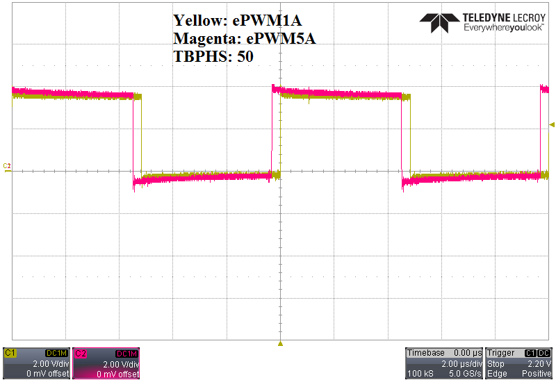
I am using the TMS320F28335 DSP to control the phaseshift between two PWM modules (i.e. ePWM1A and ePWM5A). To my understanding according to the datasheet (page 28), I set up my PWM modules such that all PWM modules are synchronized to the ePWM1 module.
What I noted is, that an increasing value in the phaseshift register moves the waveform of the PWM module. However, the direction the waveform is moved is opposite to what I actually want :D
In particular, increasing the phaseshift for ePWM5A yields a move in the waveform to the left with respect to ePWM1A. In other words, an increasing value in the TBPHS register leads to a waveforms shifted to the left with respect to the fixed ePWM1A channel. Below you'll find my code and I did some screenshots of the waveforms for two different phaseshift values to clarify my concern. I would like to achieve the opposite behavior, i.e. an increased value in the TBPHS register moves the waveform to right with respect to ePWM1A.
Do you maybe see where my misunderstanding / wrong C implementation is? Thank you for your help.
#include "DSP28x_Project.h"
#include "DCL.h"


void InitialADC();
void InitePWM1();
void InitePWM2();
void InitePWM5();
void InitePWM6();
__interrupt void ADC_isr();
__interrupt void TZ_isr();

// Flash functionality
extern Uint16 RamfuncsLoadStart;
extern Uint16 RamfuncsLoadEnd;
extern Uint16 RamfuncsRunStart;

Uint16 phaseshift;
Uint16 phaseshift1;
volatile int32 dummy;

volatile Uint16 ConversionCount;
volatile float32 Voltage1[256];
volatile float32 Current[256];

void main(void) {

	// Initialize PLL, Watchdog, enable peripheral clocks
	InitSysCtrl();

	// Used to program to flash
    MemCopy(&RamfuncsLoadStart, &RamfuncsLoadEnd, &RamfuncsRunStart);

	// Initialize ePWM and TZ
	InitEPwmGpio();
	InitTzGpio();

	// Initialize PIE control registers
	InitPieCtrl();

	IER = 0x0000;
	IFR = 0x0000;

	// Initialize PIE vector table to default ISR
	InitPieVectTable();

	// Remap the ISR function to the PIE vector table
	EALLOW;
	PieVectTable.ADCINT = &ADC_isr;
	PieVectTable.EPWM1_TZINT = &TZ_isr;
	EDIS;

	// First step of setting up the ADC sampling rate
	EALLOW;
	SysCtrlRegs.HISPCP.all = 3; // HSPCLK = SYSCLKOUT/2*ADC_MODCLK2 = 150/(2*3)   = 25.0 MHz
	EDIS;

	// Synchronization already done in the InitSysCtrl() function --> Ask the TI support to verify
	/*
	EALLOW;
	SysCtrlRegs.PCLKCR0.bit.TBCLKSYNC = 1;	// Enable time base clock synchronization with SYSCLKOUT from DSP
	EDIS;
	*/

    InitFlash();

	dummy = 0;

	// Initialize the ADC
	InitAdc();
	phaseshift1 = 4;	// Compensating a ca. 15ns delay between ePWM1 and ePWM6
	InitialADC();		// Set up the ADC for voltage and current measurement

	EALLOW;
	SysCtrlRegs.PCLKCR0.bit.TBCLKSYNC = 0;
	EDIS;

	InitePWM1();
	InitePWM2();
	InitePWM5();
	InitePWM6();

	EALLOW;
	SysCtrlRegs.PCLKCR0.bit.TBCLKSYNC = 1;
	EDIS;

	/*
	 * Set GPIO4 as output to measure execution time within ISR
	 */
	EALLOW;
	// Set GPIO10 as a GPIO - already done in InitGpio()
	GpioCtrlRegs.GPAMUX1.bit.GPIO4 = 0;
	// Set GPIO10 as an output
	GpioCtrlRegs.GPADIR.bit.GPIO4 = 1;
	EDIS;

	PieCtrlRegs.PIEIER1.bit.INTx6 = 1;	// Group 1, bit 6 for ADC
	PieCtrlRegs.PIEIER2.bit.INTx1 = 1;	// Group 2, bit 1 for ePWM1_TZ
	IER |= M_INT1;						// Sets the interrupt enable bit of group 1
	IER |= M_INT2;						// Sets the interrupt enable bit of group 3
	EINT;								// Enable global interrupts INTM

	for(;;)
	{

	}
}

__interrupt void ADC_isr(void)
{

	Voltage1[ConversionCount] = AdcRegs.ADCRESULT0 >>4;	// Read value from ADCINA5
	Current[ConversionCount] = AdcRegs.ADCRESULT1 >>4;	// Read value from ADCINB5


		EPwm5Regs.TBPHS.half.TBPHS = dummy;	// ePWM5 and ePWM6 will have phaseshift
		EPwm6Regs.TBPHS.half.TBPHS = phaseshift1;	// Compensate ca. 16ns delay of ePWM6

	      // If 256 conversions have been logged, start over
	      if(ConversionCount == 255)
	      {
	         ConversionCount = 0;
	      }
	      else
	      {
	          ConversionCount++;
	      }

		// Re-initialize for next ADC
		AdcRegs.ADCTRL2.bit.RST_SEQ1 = 1;	// Reset SEQ1
		AdcRegs.ADCST.bit.INT_SEQ1_CLR = 1;	// Clears the interrupt flag bit
		PieCtrlRegs.PIEACK.all = PIEACK_GROUP1;	// Acknowledge interrupt to PIE
}

void InitialADC(void)
{
	// Configure ADC
	AdcRegs.ADCTRL3.bit.ADCCLKPS = 1;	// Set the ADC sampling rate: 25MHz/(2*1+1) = 8.3MHz
	AdcRegs.ADCTRL1.bit.ACQ_PS = 0;		//
	AdcRegs.ADCTRL1.bit.SEQ_CASC = 0;	// Cascaded mode
	AdcRegs.ADCTRL1.bit.CONT_RUN = 0;	// Start-stop mode
	AdcRegs.ADCTRL3.bit.SMODE_SEL = 1;	// Simultaneous sampling mode
	AdcRegs.ADCTRL2.bit.EPWM_SOCA_SEQ1 = 1;	// ePWM starts SOCA trigger
	AdcRegs.ADCMAXCONV.bit.MAX_CONV1 = 0;	// One conversion
	AdcRegs.ADCCHSELSEQ1.bit.CONV00 = 5;	// ADCINA5 and ADCINB5
	AdcRegs.ADCTRL2.bit.INT_ENA_SEQ1 = 1;	// Interrupt request enabled
}

void InitePWM1(void)
{
	// Enable SOCA for ADC measurements
    EPwm1Regs.ETSEL.bit.SOCAEN = 1;            	// Enable SOCA
    EPwm1Regs.ETSEL.bit.SOCASEL = 4;            // Generate SOCA pulse at 50% duty cycle
    EPwm1Regs.ETPS.bit.SOCAPRD = 1;             // Generate pulse on 1st event

	EPwm1Regs.TBPRD = 1499;	// Set the PWM period time
	EPwm1Regs.CMPA.half.CMPA = (1499+1)/2;
	EPwm1Regs.TBPHS.half.TBPHS = 0; // Set Phase register to zero
	EPwm1Regs.TBCTL.bit.CTRMODE = TB_COUNT_UP;	// Up count mode
	EPwm1Regs.TBCTL.bit.PHSEN = TB_DISABLE; // Slave module
	EPwm1Regs.TBCTL.bit.PRDLD = TB_SHADOW;
	EPwm1Regs.TBCTL.bit.SYNCOSEL = TB_CTR_ZERO; // Sync down-stream module
	EPwm1Regs.TBCTL.bit.HSPCLKDIV = 0;	// Set time base clock to SYSCLKOUT
	EPwm1Regs.CMPCTL.bit.SHDWAMODE = CC_SHADOW;
	EPwm1Regs.CMPCTL.bit.SHDWBMODE = CC_SHADOW;
	EPwm1Regs.CMPCTL.bit.LOADAMODE = 0;	// Loads on either CTR=0 or CTR=PRD
	EPwm1Regs.CMPCTL.bit.LOADBMODE = 0;	// Loads on either CTR=0 or CTR=PRD
	EPwm1Regs.AQCTLA.bit.ZRO = AQ_SET;	// Sets pin when CTR=PRD
	EPwm1Regs.AQCTLA.bit.CAU = AQ_CLEAR;	// Clears pin when CTR=COMPA


	EPwm1Regs.DBCTL.bit.IN_MODE = 0;	// ePWMxA source for falling and rising edge
	EPwm1Regs.DBCTL.bit.OUT_MODE = DB_FULL_ENABLE;	// DB full enable
	EPwm1Regs.DBCTL.bit.POLSEL = DB_ACTV_HIC;		// Active high complementary

	EPwm1Regs.DBRED = DT;
	EPwm1Regs.DBFED = DT;
}

void InitePWM2(void)
{
	EPwm2Regs.TBPRD = 1499;	// Set the PWM period time
	EPwm2Regs.CMPA.half.CMPA = (1499+1)/2;
	EPwm2Regs.TBPHS.half.TBPHS = 0; // Set Phase register to zero
	EPwm2Regs.TBCTL.bit.CTRMODE = TB_COUNT_UP;	// Up count mode
	EPwm2Regs.TBCTL.bit.PHSEN = TB_ENABLE; // Slave module
	EPwm2Regs.TBCTL.bit.PRDLD = TB_SHADOW;
	EPwm2Regs.TBCTL.bit.SYNCOSEL = TB_CTR_ZERO; // Sync down-stream module
	EPwm2Regs.TBCTL.bit.HSPCLKDIV = 0;	// Set time base clock to SYSCLKOUT
	EPwm2Regs.CMPCTL.bit.SHDWAMODE = CC_SHADOW;
	EPwm2Regs.CMPCTL.bit.SHDWBMODE = CC_SHADOW;
	EPwm2Regs.CMPCTL.bit.LOADAMODE = 0;	// Loads on either CTR=0 or CTR=PRD
	EPwm2Regs.CMPCTL.bit.LOADBMODE = 0;	// Loads on either CTR=0 or CTR=PRD
	EPwm2Regs.AQCTLA.bit.ZRO = AQ_CLEAR;	// Clears pin when CTR=PRD
	EPwm2Regs.AQCTLA.bit.CAU = AQ_SET;	// Sets pin when CTR=COMPA

	EALLOW;
	EPwm2Regs.TZSEL.bit.OSHT3 = 1;		// Enable TZ3
	EPwm2Regs.TZCTL.bit.TZA = 2;		// Clear ePWM2A on TZ event
	EPwm2Regs.TZCTL.bit.TZB = 2;		// Clear ePWM2B on TZ event
	EDIS;

	EPwm2Regs.DBCTL.bit.IN_MODE = 0;	// ePWMxA source for falling and rising edge
	EPwm2Regs.DBCTL.bit.OUT_MODE = DB_FULL_ENABLE;	// DB full enable
	EPwm2Regs.DBCTL.bit.POLSEL = DB_ACTV_HIC;		// Active high complementary

	EPwm2Regs.DBRED = DT;
	EPwm2Regs.DBFED = DT;
}

void InitePWM5(void)
{
	EPwm5Regs.TBPRD = 1499;	// Set the PWM period time
	EPwm5Regs.CMPA.half.CMPA = (1499+1)/2;
	EPwm5Regs.TBPHS.half.TBPHS = 0; // Set Phase register to zero
	EPwm5Regs.TBCTL.bit.CTRMODE = TB_COUNT_UP;	// Up count mode
	EPwm5Regs.TBCTL.bit.PHSEN = TB_ENABLE; // Master module
	EPwm5Regs.TBCTL.bit.PRDLD = TB_SHADOW;
	EPwm5Regs.TBCTL.bit.SYNCOSEL = TB_CTR_ZERO; // Sync down-stream module
	EPwm5Regs.TBCTL.bit.HSPCLKDIV = 0;	// Set time base clock to SYSCLKOUT
	EPwm5Regs.CMPCTL.bit.SHDWAMODE = CC_SHADOW;
	EPwm5Regs.CMPCTL.bit.SHDWBMODE = CC_SHADOW;
	EPwm5Regs.CMPCTL.bit.LOADAMODE = 0;	// Loads on either CTR=0 or CTR=PRD
	EPwm5Regs.CMPCTL.bit.LOADBMODE = 0;	// Loads on either CTR=0 or CTR=PRD
	EPwm5Regs.AQCTLA.bit.ZRO = AQ_SET;	// Sets pin when CTR=PRD
	EPwm5Regs.AQCTLA.bit.CAU = AQ_CLEAR;	// Clears pin when CTR=COMPA


	EALLOW;
	EPwm5Regs.TZSEL.bit.OSHT3 = 1;		// Enable TZ3
	EPwm5Regs.TZCTL.bit.TZA = 2;		// Clear ePWM5A on TZ event
	EPwm5Regs.TZCTL.bit.TZB = 2;		// Clear ePWM5B on TZ event
	EDIS;


	EPwm5Regs.DBCTL.bit.IN_MODE = 0;	// ePWMxA source for falling and rising edge
	EPwm5Regs.DBCTL.bit.OUT_MODE = DB_FULL_ENABLE;	// DB full enable
	EPwm5Regs.DBCTL.bit.POLSEL = DB_ACTV_HIC;		// Active high complementary

	EPwm5Regs.DBRED = DT;
	EPwm5Regs.DBFED = DT;
}

void InitePWM6(void)
{
	EPwm6Regs.TBPRD = 1499;	// Set the PWM period time
	EPwm6Regs.CMPA.half.CMPA = (1499+1)/2;
	EPwm6Regs.TBPHS.half.TBPHS = 0; // Set Phase register to zero
	EPwm6Regs.TBCTL.bit.CTRMODE = TB_COUNT_UP;	// Up count mode
	EPwm6Regs.TBCTL.bit.PHSEN = TB_ENABLE; // Slave module
	EPwm6Regs.TBCTL.bit.PRDLD = TB_SHADOW;
	EPwm6Regs.TBCTL.bit.SYNCOSEL = TB_CTR_ZERO; // Sync down-stream module
	EPwm6Regs.TBCTL.bit.HSPCLKDIV = 0;	// Set time base clock to SYSCLKOUT
	EPwm6Regs.CMPCTL.bit.SHDWAMODE = CC_SHADOW;
	EPwm6Regs.CMPCTL.bit.SHDWBMODE = CC_SHADOW;
	EPwm6Regs.CMPCTL.bit.LOADAMODE = 0;	// Loads on either CTR=0 or CTR=PRD
	EPwm6Regs.CMPCTL.bit.LOADBMODE = 0;	// Loads on either CTR=0 or CTR=PRD
	EPwm6Regs.AQCTLA.bit.ZRO = AQ_CLEAR;	// Clears pin when CTR=PRD
	EPwm6Regs.AQCTLA.bit.CAU = AQ_SET;	// Sets pin when CTR=COMPA


	EALLOW;
	EPwm6Regs.TZSEL.bit.OSHT3 = 1;		// Enable TZ3
	EPwm6Regs.TZCTL.bit.TZA = 2;		// Clear ePWM6A on TZ event
	EPwm6Regs.TZCTL.bit.TZB = 2;		// Clear ePWM6B on TZ event
	EDIS;


	EPwm6Regs.DBCTL.bit.IN_MODE = 0;	// ePWMxA source for falling and rising edge
	EPwm6Regs.DBCTL.bit.OUT_MODE = DB_FULL_ENABLE;	// DB full enable
	EPwm6Regs.DBCTL.bit.POLSEL = DB_ACTV_HIC;		// Active low complementary

	EPwm6Regs.DBRED = DT;
	EPwm6Regs.DBFED = DT;
}