This thread has been locked.

If you have a related question, please click the "Ask a related question" button in the top right corner. The newly created question will be automatically linked to this question.

TMS320F28374S: ADC & GPIO internal block diagram

Part Number: TMS320F28374S

Hi Team,

  My customer is using TMS320F28374s for solar inverter application, during the usage of TMS320F28374s, there may exist some situations that the GPIO input voltage and ADC input voltage bigger than VDDIO/VDDA, they want to know the internal block diagram which help customer to predict the reliability,  could you kindly help to provide the block diagram of ADC and GPIO which  include the power supply and protection model to customer?

 Expect for your reply, thanks.

Best Regards

Benjamin

  • Benjamin,

    There are simple ESD protection diodes between the pins and their assigned power supplies. The turn-on knee voltage is around 0.7V, but as with any diode, the current will start to conduct before the knee voltage.

    For example, where GPIO > VDDIO, one ESD diode will conduct current from GPIO to VDDIO. Where GPIO < VSS, the other ESD diode will conduct current from VSS to GPIO.

    These diodes are only designed to handle singular discharge events, not sustained current conduction.

    -Tommy
  • Hi Tommy,
    What's your mean for "handle singular discharge events, not sustained current conduction"? Does it mean that while the GPIO > VDDIO or ADC input > VDDA for a while, the C2000 device should be OK? what's the timing limitation for this situation?
    Another item is that the Vih maximum value is VDDIO + 0.3V, does it mean the 0v < (GPIO - VDDIO) < 0.3V can maintain for long time?
    As customer can't avoid the situation that customer need to evaluate the risk of ADC input or GPIO input voltage bigger than VDDIO/VDDA.

    Best Regards
    Benjamin
  • Benjamin,

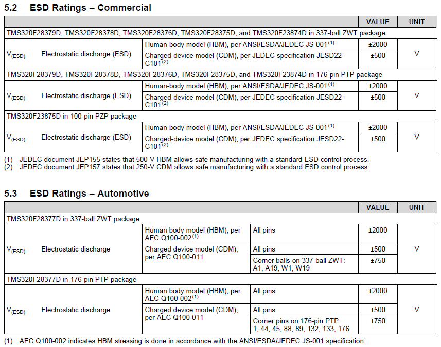
    The primary function for the protection diodes is to mitigate the ESD events specified in the datasheet:

    A side-effect of having these ESD protection diodes is that current will be conducted when the pins exceed their supply voltages.

    Both the voltage and clamp current conditions from the Absolute Maximum Ratings table must be met in order to avoid permanent damage to the ESD diodes.

    -Tommy

  • Hi Tommy,
    Worked with HUAWEI for the schematic change, currently the VDDIO can be controlled under 0.3V, what's your comment while the VDDIO will come to 0.3V while system is powered off, should be OK or not?
    Expect for your reply, thanks.

    Best Regards
    Benjamin
  • Benjamin,

    What are the states of the other supply pins when the system is powered off and VDDIO has 0.3V?  Are the IO and Analog pins isolated from outside voltage sources when powered down?  Is the system expected to be powered off in this state for a prolonged period of time?  (ex: Minutes or Hours?)

    Will VDDIO ramp up from 0.3V at power-on?

    -Tommy

  • Hi Tommy,

     1) The 3.3V are all connected together,  and 1.2V is separated;  while system powered off at night,  the 3.3V will still have 0.3V , and 1.2V will down to 0v;    

     2) The system expected to be powered off in this states for at least hours(It's solar inverter application, this states related to night);

     3)  VDDIO will ramp up from 0.3V at power-on;

     4) I'm not sure what the meaning of "Are the IO and Analog pins isolated from outside voltage sources when powered down?",  but most of the Analog PINs will have no voltage when powered down expect the ADC input sampling the PV panel voltage and AC grid Voltage.

     Will the MCU be safe while the VDDIO/VDDA and other 3.3V power supply are below 0.3V and ramp up from 0.3V?  expect for your reply, thanks.

    Best Regards

    Benjamin
  • Benjamin,

    I would not expect any issues as long as they can keep the 3.3V supplies below the ESD diode turn-on voltage (which should be met at 0.3V).

    Benjamin Zhou said:

     4) I'm not sure what the meaning of "Are the IO and Analog pins isolated from outside voltage sources when powered down?",  but most of the Analog PINs will have no voltage when powered down expect the ADC input sampling the PV panel voltage and AC grid Voltage.

    By this, I mean that the IO and Analog pins should also have external protection to make sure that external voltages greater than VDDIO & VDDA are not forced onto them so that their ESD diodes are protected.

    -Tommy