This thread has been locked.

If you have a related question, please click the "Ask a related question" button in the top right corner. The newly created question will be automatically linked to this question.

TMS320F2808: SPI Timing information

Part Number: TMS320F2808
Other Parts Discussed in Thread: ADS8319

Hello
This is a follow on question refering to post :-

According to SPRUG72, section 1.3.2.2:

“The /SPISTE pin operates as the slave-select pin. An active-low signal on the /SPISTE pin allows the slave SPI to transfer data to the serial data line; an inactive- high signal causes the slave SPI serial shift register to stop and its serial output pin to be put into the high-impedance state. This allows many slave devices to be tied together on the network, although only one slave device is selected at a time.”


It seems that the SOMI is driven high/low timed after /SPISTE transitions, rather than waiting for any clock edge after /SPISTE goes active or inactive.


I’m unable to locate any timing info for how soon one TMS320 slave disables SOMI and another TMS320 starts driving it, if we have, for example, /SPISTE to one device deselected at the same time as another is selected, as if driven from a De-multiplexer responding to ABC input changes while having the demux output permanently enabled.


I might also be interested to know how short an active pulse on an /SPISTE might have to be to rule out causing a further TMS320 to momentarily fire up it’s SOMI.


In our design, the SOMI signals from each TMS320 run through a 47 Ohm resistor before being joined together, so in the worst case both driving together to different logic levels would be done into a 94 ohm load.


Once we know the SOMI Output off and on times, we can adjust the SPI CLK relative to /SPISTE.

Best Regards

Bob Bacon

  • Hi Bob,

    As you have found, we do not document this timing. I will need to do a bit of digging to see this. Is your SPI the Master and the one driving SPISTE? 

    Thanks,

    Mark

  • Hello MArk
    This is related to e2e.ti.com/.../588531
    F2808 is the Master connected to ADS8319.
    Regards
    Bob
  • Hi Mark,

    For the SPI interface that I'm interested in, we have four TMS320 slaves (as well as other slaves) on the same SPI bus.   

    The (non TMS) SPI Master has only one SPI bus, but has four Master_SPI_CS lines, and re-configures the SPI bus each time it uses a different Master_SPI_CS.  Just one of the Master_SPI_CS signals, SPI_CS0, is used to access the set of four TMS320 slaves.

    The Master SPI_CS0 enables the output of a 2-4 line de-multiplexer that decodes a pair of signals from a very slow access port controlled by the SPI master to generate the individual TMS320 Slave SPI_CS signals.  Unless action is taken to manage the situation, the pair of de-multiplexer input signals, aren't stable until after the Master SPI_CS0 has already gone active, leading to untidy individual Slave SPI_CS active in succession as the de-multiplexer responds to input changes following being enabled.

    We are able to delay the SPI Clock to when everything is stable, so there is no issue with the data transfers but prior to that point, individual Slave SPI_CS may be unstable and the interaction of the SOMI signals from each is what I wanted to have a better understanding of, as I gather it is the individual TMS320 SPI_CS going active or inactive that starts and stops the SOMI being an active output on each device.  Hence the desire to understand the timing, and any other consequences, before I propose a SW change that there is likely to be some resistance to without a thorough analysis of the situation.

    Another aspect that I would welcome confirmation of, is that as far as I can tell, unintended, brief, SPI_CS that are not accompanied by any SPI_CLK does not lead to any processing burden at the Slave, such as any interrupt handling.  

    Thanks,

    Andy Jones

  • Hi Andy,

    I don't have those timings readily available. If you read the first quote in Bob's first message, the SOMI pin will be put into high-impedance state. meaning that the pin will be undriven. Is the pull-up enabled on the SPISOMI pin?

    I will need to ping our design team to understand the minimum SPISTE timing and understand what a glitch may do.

    If it is possible, can you share a snippet of the schematic or diagram of the full SPI network including the mux/demux and control signals.
    Additionally, can you show some timing diagrams or scope captures to illustrate the issues that you are seeing. I think I can understand what you have shared, but a diagram will be clear. Please annotate the image as necessary.

    Regards,
    Mark
  • Hi Mark,

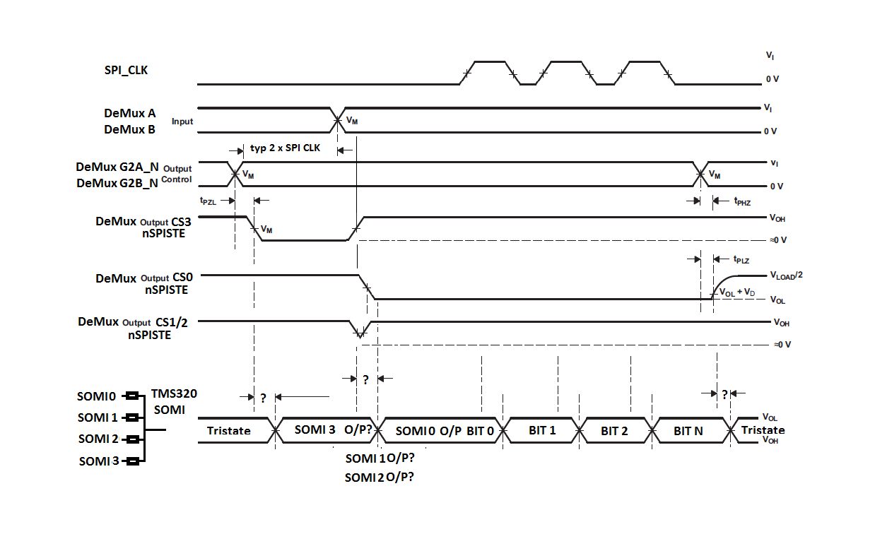
    Having run this information past tagging aware colleagues, I've excluded all company schematic and technical info to avoid any commercially sensitive data elevating the tagging from that of TI data that is widely available in the public domain. Instead, I've put together a very simple timing diagram in Paint, solely from the TI data, and If you picture a typical TI device doing the de-multiplexing, but with outputs enabled ahead of the ABC inputs being stable, then the effect on the TMS320 SOMI signals in response to individual nSPISTE changes is the area of interest.

    Best Regards

    Andy Jones

    Enclosed:

  • Hello Andy.

    Thank you for the diagram. It would be great if you could define the timings that you have labeled on the diagram. It will help me to digest it better. Are the Timings with '?'s what you are requesting? What are the Demux G2A/B_N signals? Is the master SPI driving the Demux A/B signals? 

    You said that during the reconfiguration of the mux, there is a potentially unstable period of other chip select signals that looks like it is causing unintended SOMI activity. How long is this period? What is the demux chip that is used? Can an additional signal be used to disable the outputs during reconfiguration? 

    I have requested an update from our design team on the timings that you requested. I will follow up with you tomorrow if I hear anything.

    Andrew Jones94 said:
    Another aspect that I would welcome confirmation of, is that as far as I can tell, unintended, brief, SPI_CS that are not accompanied by any SPI_CLK does not lead to any processing burden at the Slave, such as any interrupt handling.  

    No, there is interrupt handling that may potentially be triggered by a spurious SPISTE pulse and no clocks. 

    Regards,

    Mark

  • Hi Mark,

    The A and B inputs to the demux (a typical SN74LVC138) are indeed from the same processor that is generating the Demux G2A_N, G2B_N, but are configured through a discrete latch hanging off a very slow bus, un-associated with the SPI function, so can end up changing after the SPI function has been triggered, despite the executing SW setting up the port first, and then commanding an SPI transfer.

    Hopefully, you can provide times to replace the question marks (some of which may have the same answer).  This is all based on an existing design that we are on the point of taking from prototype HW to production boards, so we are trying to characterise it, and wanting to understand if this raises a problem that should be addressed by:

    • Tolerate a design with glitchy/unstable TMS320 SPISTE inputs, and defer the SPI CLK until it has all settled down (i.e. what we do now) (not especially tidy, but popular, if there are no significant consequences)
    • SW constraint to delay SPI_CS until we know the A and B inputs are stable (=unpopular)
    • HW modification (=very unpopular)
    • Extra HW control and SW to control it (= universally unpopular)
    • Any option not covered above.

    Thanks,

    Andy

  • Andy,

    The minimum delay time from SPISTE going active to SPISOMI being driven is 1.5tc(SYSCLK). This is a design simulation number, so I would add some padding on top of it. It is not a value that we have characterized across PVT.

    Additionally, any glitch on SPISTE can possibly be captured as a valid SPISTE. There is no protection here.

    It sounds like your best bet here is to delay any SPICLK transitions for sufficient time to allow the SPISTE network to stabilize- the first option on the list. As long as no clocks transitions occur during the Chip Select settling period, no C2000 SPI will latch in data. The issue here is that you may temporarily have an interesting SOMI signal if multiple slaves drive different values at the same time if their SPISTE signals are simultaneously active.

    My recommendation as an engineer would be to fix the HW to prevent the glitchy mux.

    However, I can recommend two reasonable workarounds:
    1. We do have GPIO input qualification that you could set up on SPISTE. Assuming that the glitching is not held for a very long, you could set up qualification such that the glitch will not be latched into the SPI. This would be an exaggeration, but you could set up the qualification so that the signal needs to be held for 25 SYSCLK cycles before it is recognized. You will need to ensure that the SPICLK does not toggle for at least that long after the SPISTE is driven.

    2. The other option is to kind of decouple the SPISTE from the SPI until you recognize the SPISTE is stable. So first remove SPISTE from the GPIO mux, and set up a falling edge interrupt on the GPIO. Add input qualification here as well to filter out the glitching. Once you get the GPIO interrupt, reconfigure the GPIO to be SPISTE, and then the SPI will go active. on the risiing edge of SPISTE, you can reconfigure the GPIO mux again, and then repeat.

    In both workarounds, you will need to spend some cycles in qualification, and delaying the SPICLK from driving for at least as long as the minimum glitch + GPIO Qualification + SPISTE setup time.

    Do either of these make sense?

    Thanks,
    Mark
  • Hi Mark,


    Interesting.  From SPRUG72 Figure 1-2, focussing on the SPI-relevant parts of the chip, it looked as though SPISTE possibly had an immediate effect on enabling a tri-state buffer, but it makes sense that there should be an element of SYSCLK to factor in.  Thanks for determining SPISTE to SPISOMI active time, accepting done via simulation. 


    Is it possible to determine the likely maximum time to inactive as well?


    Thanks for confirming that delaying the SPICLK transitions until after the SPISTE has stabilised is advised, as we do.  I think that will be the approach that we will retain.


    I agree that the design could be improved, but as you have demonstrated, we are used to having to accept something that offers at least one workable compromises.


    I like both of your other workaround ideas.  Am I right in thinking that the SPISTE input qualification to supress glitches would effectively delay the SPISOMI going active, and, at the end, inactive?  I hadn’t considered using that facility except on GPIO pins used as GPIO.

    Would it be viable to have longer input qualification on SPISTE until it was active, and then turn off the qualification for that input while the SPISTE was active, without affecting the SPI in progress, if we wanted to?


    I can see that the second method would work well too.  It is always nice to know there are other solutions to fall back on, but I expect on this occasion, we will leave the TMS320 code as is, and try to improve our management of signals to our TMS320s.


    Thanks,


    Andy

  • Andy,

     Figure 1-2 of SPRUG72 is a pretty detailed diagram as far as a high-level diagrams go. It is not an exact implementation diagram, so things like syncronizers and signal buffers are not present.  I will need to look at the delay time from SPISTE inactive to SPISOMI hiZ as well.

    Having the input qualification on the SPISTE will effectively delay the Start and end of the SPISOMI active state. The nice thing about the SPISTE is that it should not be driven at a high frequency, so you should not need to change the input qualification during the active transmission. it will just delay the activity. There will not be any glitching on the GPIO if you choose to change input qualification during the transmission, but it will be extra SW to manage. If you need to recover some time in the system, and can eat some device clock cycles to actively manage the qualification, I don't have any problems with this.

    -Mark