This thread has been locked.
If you have a related question, please click the "Ask a related question" button in the top right corner. The newly created question will be automatically linked to this question.
Hi all,
I try to implement peak current mode control with the TMS320F28379D.
A 1V signal is applied to the CMPIN1P Pin. The ramp generator is used on the negative input of the comparator. The CMPSS Module 1 is configured with the following code:
CMPSS_enableModule(CMPSS1_BASE); CMPSS_configHighComparator(CMPSS1_BASE, CMPSS_INSRC_DAC); CMPSS_configDAC(CMPSS1_BASE, CMPSS_DACVAL_PWMSYNC | CMPSS_DACREF_VDDA | CMPSS_DACSRC_RAMP); CMPSS_configOutputsHigh(CMPSS1_BASE, CMPSS_TRIP_FILTER | CMPSS_TRIPOUT_SYNC_COMP); CMPSS_setRampDecValue(CMPSS1_BASE, RAMP_DECREMENT); CMPSS_setRampDelayValue(CMPSS1_BASE, RAMP_DELAY); CMPSS_configRamp(CMPSS1_BASE, 27000, RAMP_DECREMENT, RAMP_DELAY, 1, true); CMPSS_configFilterHigh(CMPSS1_BASE, 2, 20, 15); CMPSS_initFilterHigh(CMPSS1_BASE);
GPIO_setMasterCore(11, GPIO_CORE_CPU1);
GPIO_setPinConfig(GPIO_11_OUTPUTXBAR7);
GPIO_setDirectionMode(11, GPIO_DIR_MODE_OUT);
GPIO_setPadConfig(11, GPIO_PIN_TYPE_STD);
XBAR_setOutputMuxConfig(XBAR_OUTPUT7, XBAR_OUT_MUX00_CMPSS1_CTRIPOUTH);
XBAR_enableOutputMux(XBAR_OUTPUT7, XBAR_MUX00); XBAR_setEPWMMuxConfig(XBAR_TRIP4, XBAR_EPWM_MUX00_CMPSS1_CTRIPH); XBAR_enableEPWMMux(XBAR_TRIP4, XBAR_MUX00);
This works as expected.
Now there are two options to configure the ePWM module.
Option1: The traditional way using the Trip Zone, same as with the old ePWM Type 1
// Set-up TBCLK EPWM_setTimeBasePeriod(EPWM1_BASE, PWM_TIMER_TBPRD); EPWM_setPhaseShift(EPWM1_BASE, 0); EPWM_setTimeBaseCounter(EPWM1_BASE, 0U); EPWM_setSyncOutPulseMode(EPWM1_BASE, EPWM_SYNC_OUT_PULSE_ON_COUNTER_ZERO); // Set up counter mode EPWM_setTimeBaseCounterMode(EPWM1_BASE, EPWM_COUNTER_MODE_UP); EPWM_disablePhaseShiftLoad(EPWM1_BASE); EPWM_setClockPrescaler(EPWM1_BASE, EPWM_CLOCK_DIVIDER_1, EPWM_HSCLOCK_DIVIDER_1); // Set up shadowing EPWM_setCounterCompareShadowLoadMode(EPWM1_BASE, EPWM_COUNTER_COMPARE_A, EPWM_COMP_LOAD_ON_CNTR_ZERO); EPWM_setCounterCompareShadowLoadMode(EPWM1_BASE, EPWM_COUNTER_COMPARE_B, EPWM_COMP_LOAD_ON_CNTR_ZERO); // Set Compare values EPWM_setCounterCompareValue(EPWM1_BASE, EPWM_COUNTER_COMPARE_A, 0); // Set actions EPWM_setActionQualifierAction(EPWM1_BASE, EPWM_AQ_OUTPUT_A, EPWM_AQ_OUTPUT_HIGH, EPWM_AQ_OUTPUT_ON_TIMEBASE_ZERO); EPWM_setActionQualifierAction(EPWM1_BASE, EPWM_AQ_OUTPUT_A, EPWM_AQ_OUTPUT_LOW, EPWM_AQ_OUTPUT_ON_TIMEBASE_UP_CMPA); // Set Digital Compare // TRIP4 -> DCBH EPWM_enableDigitalCompareTripCombinationInput(EPWM1_BASE, EPWM_DC_COMBINATIONAL_TRIPIN4, EPWM_DC_TYPE_DCBH); // DCBH -> DCBEVT2 EPWM_setTripZoneDigitalCompareEventCondition(EPWM1_BASE, EPWM_TZ_DC_OUTPUT_B2, EPWM_TZ_EVENT_DCXH_HIGH); // Enable DCB as CBC EPWM_enableTripZoneSignals(EPWM1_BASE, EPWM_TZ_SIGNAL_DCBEVT2); // Set Trip Zone EPWM_setTripZoneAction(EPWM1_BASE, EPWM_TZ_ACTION_EVENT_TZA, EPWM_TZ_ACTION_LOW);
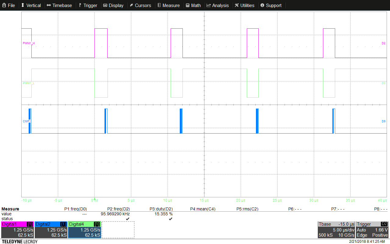
This works as expected. When the Cmpss1Regs.RAMPMAXREFS value is increased linear from 0 to 40000, the PWM is low at the beginning and as soon as the ramp start value crosses the 1V small PWM pulses are generated.
The scope shot shows the Duty Cycle rises from 0 to 25%. With the comparator pulse, the PWM turns low. Everything works as expected.
Footnote: PWM1_L is permanent low. This should be the inverted signal of PWM1_H, but is not possible with the DSP. The inversion and dead band will be generated externally with a hardware gate.
Option2: The new way using the Action Quallifier and the Dead Band
Instead of using the Trip Zone to clear the PWM signal the Action Qualifier is used. This has the advantage of generation the complementary PWM signal with the Dead Band module.
// Set-up TBCLK EPWM_setTimeBasePeriod(EPWM1_BASE, PWM_TIMER_TBPRD); EPWM_setTimeBaseCounter(EPWM1_BASE, 0U); EPWM_setSyncOutPulseMode(EPWM1_BASE, EPWM_SYNC_OUT_PULSE_ON_COUNTER_ZERO); // Set up counter mode EPWM_setTimeBaseCounterMode(EPWM1_BASE, EPWM_COUNTER_MODE_UP); EPWM_disablePhaseShiftLoad(EPWM1_BASE); EPWM_setClockPrescaler(EPWM1_BASE, EPWM_CLOCK_DIVIDER_1, EPWM_HSCLOCK_DIVIDER_1); // Set up shadowing EPWM_setCounterCompareShadowLoadMode(EPWM1_BASE, EPWM_COUNTER_COMPARE_A, EPWM_COMP_LOAD_ON_CNTR_ZERO); EPWM_setCounterCompareShadowLoadMode(EPWM1_BASE, EPWM_COUNTER_COMPARE_B, EPWM_COMP_LOAD_ON_CNTR_ZERO); // Set Compare values EPWM_setCounterCompareValue(EPWM1_BASE, EPWM_COUNTER_COMPARE_A, 0); // Set Deadband EPWM_setDeadBandDelayPolarity(EPWM1_BASE, EPWM_DB_FED, EPWM_DB_POLARITY_ACTIVE_LOW); EPWM_setDeadBandDelayMode(EPWM1_BASE, EPWM_DB_RED, true); EPWM_setDeadBandDelayMode(EPWM1_BASE, EPWM_DB_FED, true); EPWM_setRisingEdgeDelayCount(EPWM1_BASE, PWM_DB); EPWM_setFallingEdgeDelayCount(EPWM1_BASE, PWM_DB); // Set actions EPWM_setActionQualifierAction(EPWM1_BASE, EPWM_AQ_OUTPUT_A, EPWM_AQ_OUTPUT_HIGH, EPWM_AQ_OUTPUT_ON_TIMEBASE_ZERO); EPWM_setActionQualifierAction(EPWM1_BASE, EPWM_AQ_OUTPUT_A, EPWM_AQ_OUTPUT_LOW, EPWM_AQ_OUTPUT_ON_TIMEBASE_UP_CMPA); // Set Digital Compare // TRIP4 -> DCBH EPWM_enableDigitalCompareTripCombinationInput(EPWM1_BASE, EPWM_DC_COMBINATIONAL_TRIPIN4, EPWM_DC_TYPE_DCBH); // DCBH -> DCBEVT2 EPWM_setTripZoneDigitalCompareEventCondition(EPWM1_BASE, EPWM_TZ_DC_OUTPUT_B2, EPWM_TZ_EVENT_DCXH_HIGH); // Enable DCB as T1 Source EPWM_setActionQualifierT1TriggerSource(EPWM1_BASE, EPWM_AQ_TRIGGER_EVENT_TRIG_DCB_2); EPWM_setActionQualifierAction(EPWM1_BASE, EPWM_AQ_OUTPUT_A, EPWM_AQ_OUTPUT_LOW, EPWM_AQ_OUTPUT_ON_T1_COUNT_UP);
The COMPSS1 initialization code is the same as with the option 1.
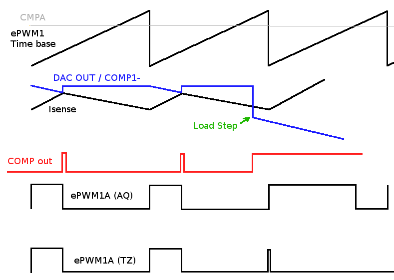
With this implementation, I have two unexpected behavior.
1: When the Ramp Start Value is below the 1V of the negative Input of the comparator, why is the duty cycle at 50% (this is the value of CMPA). My understanding is, it should be 0.
2: The Dead Band module is not generating the inverted gate signal. The Dead Band module should be independent of the Action Qualifier module.
Regards,
Tobias
As a simple test, I changed the DCBL[OUTSWAP] bits from 0b00 to 0b11. The polarity of the PWM signal changed only after the start value of the ramp was above the negative input of the comparator (last picture after ~11.3ms). Before that the PWM signal was exactly the same as without the change. This indicates to me something happens in the Trip Zone Module.
Tobias,
You should be able to use method two to develop a complementary waveform.
I'm sorry I don't think I know enough about the configuration and execution state of your device by looking at the graphs. Can you debug the device in system? I would suggest reading the PWM configuration before the comparator trips, something appears wrong. Are you setting up the rest of the PWM configuration after the first comparator trip?
Try removing the comparator portion of the code and correctly configuring the PWM, note if you turn on the PWM before it's fully configured you will get a weird output.
Regards,
Cody
Cody,
My code is based on the cmpss_ex1_asynch sample code of the driver library. The main looks like this:
void main(void) { Device_init(); Device_initGPIO(); Interrupt_initModule(); Interrupt_initVectorTable(); SysCtl_disablePeripheral(SYSCTL_PERIPH_CLK_TBCLKSYNC); InitPWMGPIO(); InitEPWM1(); SysCtl_enablePeripheral(SYSCTL_PERIPH_CLK_TBCLKSYNC); InitCMP1(); EINT; ERTM; while(1) { } }
The initCMP1 code is exactly like the one above. The InitPWM code is the same as above plus an additional interrupt is enabled:
EPWM_enableInterrupt(EPWM1_BASE); EPWM_setInterruptSource(EPWM1_BASE, EPWM_INT_TBCTR_U_CMPC); Interrupt_enable(INT_EPWM1); Interrupt_register(INT_EPWM1, &ISRPreControlTask); EPWM_setInterruptEventCount(EPWM1_BASE, 1); EPWM_clearEventTriggerInterruptFlag(EPWM1_BASE); Interrupt_clearACKGroup(INTERRUPT_ACK_GROUP3);
and the interrupt code looks like
__interrupt void ISRPreControlTask(void) { rampstart = __fmin(rampstart + DVID, __fmax(rampstart,rampstartref)); rampstart = __fmax(rampstart - DVID, __fmin(rampstart,rampstartref)); CMPSS_setMaxRampValue(CMPSS1_BASE, (uint32_t)rampstart); EPWM_clearEventTriggerInterruptFlag(EPWM1_BASE); Interrupt_clearACKGroup(INTERRUPT_ACK_GROUP3); }
I load the code to the C2000 and start it. Afterwards I set the rampstartref to 60000 in the expression window in CCS and the interrupt increases the Cmpss1Regs.RAMPMAXREFS value from 0 to 60000 linearly.
In the attachment is the source code. As hardware I use a Controlcard doking station R4.1 the scope is connected to pin 49,51(PWM) and 63 (CMPoutput). In addition a 1V source is connected to pin15 (Ain2).
//############################################################################# // // FILE: cmpss_ex1_asynch.c // // TITLE: CMPSS Asynchronous Trip // //! \addtogroup driver_example_list //! <h1> CMPSS Asynchronous Trip </h1> //! //! This example enables the CMPSS1 COMPH comparator and feeds the asynchronous //! CTRIPOUTH signal to the GPIO14/OUTPUTXBAR3 pin and CTRIPH to GPIO15/EPWM8B. //! //! \b External \b Connections \n //! - Outputs can be observed on GPIO14 and GPIO15 //! - Comparator input pin is on ADCINA2 //! //! \b Watch \b Variables \n //! - None //! // //############################################################################# // $TI Release: F2837xD Support Library v3.03.00.00 $ // $Release Date: Thu Dec 7 18:51:32 CST 2017 $ // $Copyright: // Copyright (C) 2013-2017 Texas Instruments Incorporated - http://www.ti.com/ // // Redistribution and use in source and binary forms, with or without // modification, are permitted provided that the following conditions // are met: // // Redistributions of source code must retain the above copyright // notice, this list of conditions and the following disclaimer. // // Redistributions in binary form must reproduce the above copyright // notice, this list of conditions and the following disclaimer in the // documentation and/or other materials provided with the // distribution. // // Neither the name of Texas Instruments Incorporated nor the names of // its contributors may be used to endorse or promote products derived // from this software without specific prior written permission. // // THIS SOFTWARE IS PROVIDED BY THE COPYRIGHT HOLDERS AND CONTRIBUTORS // "AS IS" AND ANY EXPRESS OR IMPLIED WARRANTIES, INCLUDING, BUT NOT // LIMITED TO, THE IMPLIED WARRANTIES OF MERCHANTABILITY AND FITNESS FOR // A PARTICULAR PURPOSE ARE DISCLAIMED. IN NO EVENT SHALL THE COPYRIGHT // OWNER OR CONTRIBUTORS BE LIABLE FOR ANY DIRECT, INDIRECT, INCIDENTAL, // SPECIAL, EXEMPLARY, OR CONSEQUENTIAL DAMAGES (INCLUDING, BUT NOT // LIMITED TO, PROCUREMENT OF SUBSTITUTE GOODS OR SERVICES; LOSS OF USE, // DATA, OR PROFITS; OR BUSINESS INTERRUPTION) HOWEVER CAUSED AND ON ANY // THEORY OF LIABILITY, WHETHER IN CONTRACT, STRICT LIABILITY, OR TORT // (INCLUDING NEGLIGENCE OR OTHERWISE) ARISING IN ANY WAY OUT OF THE USE // OF THIS SOFTWARE, EVEN IF ADVISED OF THE POSSIBILITY OF SUCH DAMAGE. // $ //############################################################################# // // Included Files // #include "driverlib.h" #include "device.h" // 20MHz XTAL on controlCARD. For use with SysCtl_getClock(). #define DEVICE_OSCSRC_FREQ 20000000U // Define to pass to SysCtl_setClock(). Will configure the clock as follows: // PLLSYSCLK = 20MHz (XTAL_OSC) * 20 (IMULT) * 1 (FMULT) / 2 (PLLCLK_BY_2) #define DEVICE_SETCLOCK_CFG (SYSCTL_OSCSRC_XTAL | SYSCTL_IMULT(20) | \ SYSCTL_FMULT_NONE | SYSCTL_SYSDIV(2) | \ SYSCTL_PLL_ENABLE) // 200MHz SYSCLK frequency based on the above DEVICE_SETCLOCK_CFG. Update the // code below if a different clock configuration is used! #define DEVICE_SYSCLK_FREQ ((DEVICE_OSCSRC_FREQ * 20 * 1) / 2) // 100MHz PWMCLK frequency based on the above DEVICE_SYSCLK_FREQ and a // pwm clock divider of 2. Update the code below if a // different EPWMCLKDIV divider is used! #define DEVICE_PWMCLK_FREQ (DEVICE_SYSCLK_FREQ / 2) // Macro to call SysCtl_delay() to achieve a delay in microseconds. The macro // will convert the desired delay in microseconds to the count value expected // by the function. \b x is the number of microseconds to delay. #define DEVICE_DELAY_US(x) SysCtl_delay(((((long double)(x)) / (1000000.0L / \ (long double)DEVICE_SYSCLK_FREQ)) - 9.0L) / 5.0L) #define PWM_FREQ 96000 #define PWM_DEAD_BAND_NS 150 #define PWM_TIMER_TBPRD (int)((DEVICE_PWMCLK_FREQ/PWM_FREQ)) #define PWM_TIMER_CMP PWM_TIMER_TBPRD/2 //#define PWM_DB (int)(PWM_DEAD_BAND_NS/(2000000000.0L/DEVICE_SYSCLK_FREQ)) #define PWM_DB 100 #define DVID 10 // 1000V/s : 1000V / 96kHz #define RAMP_DECREMENT 20 #define RAMP_DELAY 0 float rampstart = 0.0; float rampstartref = 0.0; static inline void InitPWMGPIO(void); static inline void InitEPWM1(void); static inline void InitCMP1(void); __interrupt void ISRPreControlTask(void); // // Main // void main(void) { // // Initialize device clock and peripherals // Device_init(); // // Disable pin locks and enable internal pullups. // Device_initGPIO(); // // Initialize PIE and clear PIE registers. Disables CPU interrupts. // Interrupt_initModule(); // // Initialize the PIE vector table with pointers to the shell Interrupt // Service Routines (ISR). // Interrupt_initVectorTable(); // Disable sync(Freeze clock to PWM as well) SysCtl_disablePeripheral(SYSCTL_PERIPH_CLK_TBCLKSYNC); InitPWMGPIO(); InitEPWM1(); // Enable sync and clock to PWM SysCtl_enablePeripheral(SYSCTL_PERIPH_CLK_TBCLKSYNC); InitCMP1(); // Buck Phase 1 // // Enable Global Interrupt (INTM) and realtime interrupt (DBGM) // EINT; ERTM; // // Loop indefinitely // while(1) { } } static inline void InitPWMGPIO(void) { // GPIO4 is the EPWM3A pin. GPIO_setMasterCore(0, GPIO_CORE_CPU1); GPIO_setPinConfig(GPIO_0_EPWM1A); GPIO_setDirectionMode(0, GPIO_DIR_MODE_OUT); GPIO_setPadConfig(0, GPIO_PIN_TYPE_STD); // GPIO5 is the GPIO pin. GPIO_setMasterCore(1, GPIO_CORE_CPU1); GPIO_setPinConfig(GPIO_1_EPWM1B); GPIO_setDirectionMode(1, GPIO_DIR_MODE_OUT); GPIO_setPadConfig(1, GPIO_PIN_TYPE_STD); // GPIO8 is the EPWM5A pin. GPIO_setMasterCore(8, GPIO_CORE_CPU1); GPIO_setPinConfig(GPIO_8_EPWM5A); GPIO_setDirectionMode(8, GPIO_DIR_MODE_OUT); GPIO_setPadConfig(8, GPIO_PIN_TYPE_STD); } static inline void InitEPWM1(void) { // Set-up TBCLK EPWM_setTimeBasePeriod(EPWM1_BASE, PWM_TIMER_TBPRD); //EPWM_setPhaseShift(EPWM3_BASE, 0); //EPWM_enablePhaseShiftLoad(EPWM3_BASE); EPWM_setTimeBaseCounter(EPWM1_BASE, 0U); EPWM_setSyncOutPulseMode(EPWM1_BASE, EPWM_SYNC_OUT_PULSE_ON_COUNTER_ZERO); // Set up counter mode EPWM_setTimeBaseCounterMode(EPWM1_BASE, EPWM_COUNTER_MODE_UP); EPWM_disablePhaseShiftLoad(EPWM1_BASE); EPWM_setClockPrescaler(EPWM1_BASE, EPWM_CLOCK_DIVIDER_1, EPWM_HSCLOCK_DIVIDER_1); EPWM_setCounterCompareValue(EPWM1_BASE, EPWM_COUNTER_COMPARE_A, 700); // Set up shadowing EPWM_setCounterCompareShadowLoadMode(EPWM1_BASE, EPWM_COUNTER_COMPARE_A, EPWM_COMP_LOAD_ON_CNTR_ZERO); EPWM_setCounterCompareShadowLoadMode(EPWM1_BASE, EPWM_COUNTER_COMPARE_B, EPWM_COMP_LOAD_ON_CNTR_ZERO); // Set Compare values EPWM_setCounterCompareValue(EPWM1_BASE, EPWM_COUNTER_COMPARE_A, 700); EPWM_setCounterCompareValue(EPWM1_BASE, EPWM_COUNTER_COMPARE_C, 800); // Set Deadband EPWM_setDeadBandDelayPolarity(EPWM1_BASE, EPWM_DB_FED, EPWM_DB_POLARITY_ACTIVE_LOW); EPWM_setDeadBandDelayMode(EPWM1_BASE, EPWM_DB_RED, true); EPWM_setDeadBandDelayMode(EPWM1_BASE, EPWM_DB_FED, true); EPWM_setRisingEdgeDelayCount(EPWM1_BASE, PWM_DB); EPWM_setFallingEdgeDelayCount(EPWM1_BASE, PWM_DB); // Set actions EPWM_setActionQualifierAction(EPWM1_BASE, EPWM_AQ_OUTPUT_A, EPWM_AQ_OUTPUT_HIGH, EPWM_AQ_OUTPUT_ON_TIMEBASE_ZERO); EPWM_setActionQualifierAction(EPWM1_BASE, EPWM_AQ_OUTPUT_A, EPWM_AQ_OUTPUT_LOW, EPWM_AQ_OUTPUT_ON_TIMEBASE_UP_CMPA); // Set Digital Compare // TRIP4 -> DCBH EPWM_enableDigitalCompareTripCombinationInput(EPWM1_BASE, EPWM_DC_COMBINATIONAL_TRIPIN4, EPWM_DC_TYPE_DCBH); // DCBH -> DCBEVT2 EPWM_setTripZoneDigitalCompareEventCondition(EPWM1_BASE, EPWM_TZ_DC_OUTPUT_B2, EPWM_TZ_EVENT_DCXH_HIGH); // Enable DCB as T1 Source EPWM_setActionQualifierT1TriggerSource(EPWM1_BASE, EPWM_AQ_TRIGGER_EVENT_TRIG_DCB_2); EPWM_setActionQualifierAction(EPWM1_BASE, EPWM_AQ_OUTPUT_A, EPWM_AQ_OUTPUT_LOW, EPWM_AQ_OUTPUT_ON_T1_COUNT_UP); EPWM_enableInterrupt(EPWM1_BASE); EPWM_setInterruptSource(EPWM1_BASE, EPWM_INT_TBCTR_U_CMPC); Interrupt_enable(INT_EPWM1); Interrupt_register(INT_EPWM1, &ISRPreControlTask); EPWM_setInterruptEventCount(EPWM1_BASE, 1); EPWM_clearEventTriggerInterruptFlag(EPWM1_BASE); Interrupt_clearACKGroup(INTERRUPT_ACK_GROUP3); } static inline void InitCMP1(void) { CMPSS_enableModule(CMPSS1_BASE); CMPSS_configHighComparator(CMPSS1_BASE, CMPSS_INSRC_DAC); CMPSS_configDAC(CMPSS1_BASE, CMPSS_DACVAL_PWMSYNC | CMPSS_DACREF_VDDA | CMPSS_DACSRC_RAMP); CMPSS_configOutputsHigh(CMPSS1_BASE, CMPSS_TRIP_FILTER | CMPSS_TRIPOUT_SYNC_COMP); CMPSS_setRampDecValue(CMPSS1_BASE, RAMP_DECREMENT); CMPSS_setRampDelayValue(CMPSS1_BASE, RAMP_DELAY); CMPSS_configRamp(CMPSS1_BASE, 27000, RAMP_DECREMENT, RAMP_DELAY, 1, false); CMPSS_configFilterHigh(CMPSS1_BASE, 2, 20, 15); CMPSS_initFilterHigh(CMPSS1_BASE); GPIO_setMasterCore(11, GPIO_CORE_CPU1); GPIO_setPinConfig(GPIO_11_OUTPUTXBAR7); GPIO_setDirectionMode(11, GPIO_DIR_MODE_OUT); GPIO_setPadConfig(11, GPIO_PIN_TYPE_STD); XBAR_setOutputMuxConfig(XBAR_OUTPUT7, XBAR_OUT_MUX00_CMPSS1_CTRIPOUTH); XBAR_enableOutputMux(XBAR_OUTPUT7, XBAR_MUX00); XBAR_setEPWMMuxConfig(XBAR_TRIP4, XBAR_EPWM_MUX00_CMPSS1_CTRIPH); XBAR_enableEPWMMux(XBAR_TRIP4, XBAR_MUX00); } __interrupt void ISRPreControlTask(void) { rampstart = __fmin(rampstart + DVID, __fmax(rampstart,rampstartref)); rampstart = __fmax(rampstart - DVID, __fmin(rampstart,rampstartref)); CMPSS_setMaxRampValue(CMPSS1_BASE, (uint32_t)rampstart); EPWM_clearEventTriggerInterruptFlag(EPWM1_BASE); Interrupt_clearACKGroup(INTERRUPT_ACK_GROUP3); }
I tried also move the InitCMP1 above the InitEPWM1. This doesn't change anything.
The content of the epwm registers before the rampmaxrefs is increased is:
TBCTL 0x0010 Time Base Control Register [Memory Mapped] TBCTL2 0x0000 Time Base Control Register 2 [Memory Mapped] TBCTR 0x03E4 Time Base Counter Register [Memory Mapped] TBSTS 0x0003 Time Base Status Register [Memory Mapped] CMPCTL 0x0000 Counter Compare Control Register [Memory Mapped] CMPCTL2 0x0000 Counter Compare Control Register 2 [Memory Mapped] DBCTL 0x000B Dead-Band Generator Control Register [Memory Mapped] DBCTL2 0x0000 Dead-Band Generator Control Register 2 [Memory Mapped] AQCTL 0x0000 Action Qualifier Control Register [Memory Mapped] AQTSRCSEL 0x0003 Action Qualifier Trigger Event Source Select Register [Memory Mapped] PCCTL 0x0000 PWM Chopper Control Register [Memory Mapped] HRCNFG 0x0000 HRPWM Configuration Register [Memory Mapped] HRPWR 0x0000 HRPWM Power Register [Memory Mapped] HRMSTEP 0x0000 HRPWM MEP Step Register [Memory Mapped] HRCNFG2 0x0000 HRPWM Configuration 2 Register [Memory Mapped] HRPCTL 0x0000 High Resolution Period Control Register [Memory Mapped] TRREM 0x0000 Translator High Resolution Remainder Register [Memory Mapped] GLDCTL 0x0000 Global PWM Load Control Register [Memory Mapped] GLDCFG 0x0000 Global PWM Load Config Register [Memory Mapped] EPWMXLINK 0x00000000 EPWMx Link Register [Memory Mapped] AQCTLA 0x0012 Action Qualifier Control Register For Output A [Memory Mapped] AQCTLA2 0x0001 Additional Action Qualifier Control Register For Output A [Memory Mapped] AQCTLB 0x0000 Action Qualifier Control Register For Output B [Memory Mapped] AQCTLB2 0x0000 Additional Action Qualifier Control Register For Output B [Memory Mapped] AQSFRC 0x0000 Action Qualifier Software Force Register [Memory Mapped] AQCSFRC 0x0000 Action Qualifier Continuous S/W Force Register [Memory Mapped] DBREDHR 0x0000 Dead-Band Generator Rising Edge Delay High Resolution Mirror Register [Memory Mapped] DBRED 0x0064 Dead-Band Generator Rising Edge Delay High Resolution Mirror Register [Memory Mapped] DBFEDHR 0x0000 Dead-Band Generator Falling Edge Delay High Resolution Register [Memory Mapped] DBFED 0x0064 Dead-Band Generator Falling Edge Delay Count Register [Memory Mapped] TBPHS 0x00000000 Time Base Phase High [Memory Mapped] TBPRDHR 0x0000 Time Base Period High Resolution Register [Memory Mapped] TBPRD 0x0411 Time Base Period Register [Memory Mapped] CMPA 0x02BC0000 Counter Compare A Register [Memory Mapped] CMPB 0x00000000 Compare B Register [Memory Mapped] CMPC 0x0320 Counter Compare C Register [Memory Mapped] CMPD 0x0000 Counter Compare D Register [Memory Mapped] GLDCTL2 0x0000 Global PWM Load Control Register 2 [Memory Mapped] TZSEL 0x0000 Trip Zone Select Register [Memory Mapped] TZDCSEL 0x0400 Trip Zone Digital Comparator Select Register [Memory Mapped] TZCTL 0x0000 Trip Zone Control Register [Memory Mapped] TZCTL2 0x0000 Additional Trip Zone Control Register [Memory Mapped] TZCTLDCA 0x0000 Trip Zone Control Register Digital Compare A [Memory Mapped] TZCTLDCB 0x0000 Trip Zone Control Register Digital Compare B [Memory Mapped] TZEINT 0x0000 Trip Zone Enable Interrupt Register [Memory Mapped] TZFLG 0x0040 Trip Zone Flag Register [Memory Mapped] TZCBCFLG 0x0000 Trip Zone CBC Flag Register [Memory Mapped] TZOSTFLG 0x0000 Trip Zone OST Flag Register [Memory Mapped] TZCLR 0x0000 Trip Zone Clear Register [Memory Mapped] TZCBCCLR 0x0000 Trip Zone CBC Clear Register [Memory Mapped] TZOSTCLR 0x0000 Trip Zone OST Clear Register [Memory Mapped] TZFRC 0x0000 Trip Zone Force Register [Memory Mapped] ETSEL 0x004C Event Trigger Selection Register [Memory Mapped] ETPS 0x0010 Event Trigger Pre-Scale Register [Memory Mapped] ETFLG 0x0000 Event Trigger Flag Register [Memory Mapped] ETCLR 0x0000 Event Trigger Clear Register [Memory Mapped] ETFRC 0x0000 Event Trigger Force Register [Memory Mapped] ETINTPS 0x0001 Event-Trigger Interrupt Pre-Scale Register [Memory Mapped] ETSOCPS 0x0000 Event-Trigger SOC Pre-Scale Register [Memory Mapped] ETCNTINITCTL 0x0000 Event-Trigger Counter Initialization Control Register [Memory Mapped] ETCNTINIT 0x0000 Event-Trigger Counter Initialization Register [Memory Mapped] DCTRIPSEL 0x0F00 Digital Compare Trip Select Register [Memory Mapped] DCACTL 0x0000 Digital Compare A Control Register [Memory Mapped] DCBCTL 0x0000 Digital Compare B Control Register [Memory Mapped] DCFCTL 0x0000 Digital Compare Filter Control Register [Memory Mapped] DCCAPCTL 0x0000 Digital Compare Capture Control Register [Memory Mapped] DCFOFFSET 0x0000 Digital Compare Filter Offset Register [Memory Mapped] DCFOFFSETCNT 0x0000 Digital Compare Filter Offset Counter Register [Memory Mapped] DCFWINDOW 0x0000 Digital Compare Filter Window Register [Memory Mapped] DCFWINDOWCNT 0x0000 Digital Compare Filter Window Counter Register [Memory Mapped] DCCAP 0x0000 Digital Compare Counter Capture Register [Memory Mapped] DCAHTRIPSEL 0x0000 Digital Compare AH Trip Select [Memory Mapped] DCALTRIPSEL 0x0000 Digital Compare AL Trip Select [Memory Mapped] DCBHTRIPSEL 0x0008 Digital Compare BH Trip Select [Memory Mapped] DCBLTRIPSEL 0x0000 Digital Compare BL Trip Select [Memory Mapped]
Tobias,
Regards,
Cody
Hi Cody,
1. The last scope shot above shows the comparator 1 output (blue curve). Bottom part of the split screen shows the zoomed in traces. When the negative input of the comparator is way below the 1V of the positive input of the comparator the output is permanent high. When the negative input is slightly above the 1V, the comp output goes low for a small periode. In both cases the PWM is not going low at the beginning of the PWM cycle.
2. The trip zone is not in use. Everything is disabled
TZSEL 0x0000 all One-Shot and CBC Trip sources are disabled
TZDCSEL 0x0400 DCBH = high, DCBL = don't care, all others are disabled
TZCTL 0x0000 High-impedance, but shouldn't make any difference, since the events are disabled in the TZSEL register
TZCTL2 0x0000 TZControl 2 not enabled
TZCTLDCA 0x0000 High-impedance, but shouldn't make any difference, since the events are disabled in the TZSEL register
TZCTLDCB 0x0000 High-impedance, but shouldn't make any difference, since the events are disabled in the TZSEL register
TZEINT 0x0000 no interrupt is enabled
After changing the TZCTL, TZCTLDCA and TZCTLDCB from High-impedance to do nothing, the inverted EPWM1B appears.
The first issue is resolved. Now the EPWMB is the complementary of EPWMA in all cases. Why does the TZCTL settings make a difference, even when the trip source isn't enabled?
The remaining question is, why is the action qualifier T1 not working when the comparator output is permanent high?
Regards,
Tobias
Hi Cody,
I do get the idea of using the trip zone to force the pwm low. This works as expected and was used in the earlier DSP versions. This has the disadvantage of generating the dead band externally. Since you improved the epwm module, I was eager to try the new concept of using the action qualifier. This leads to more flexibility since i can use the internal dead band an can adjust it by software.
Now back to the issue. I checked the register and the only difference is in the TZCTL, TZCTRLDCA and TZCTRLDCB registers, since i changed it from hi-impedance to do nothing.
Were you able to reproduce the issue on your board?
Regards,
Tobias
Tobias,
I was unable to reproduce your issue, could you attach your project?
Regards,
Cody
Tobias,
you are close on your implementation. You need to configure DCA and DCB to force the PWM low using the trip-zone. Something like the code below should help you.
// Set Digital Compare // TRIP4 -> DCBH EPWM_enableDigitalCompareTripCombinationInput(EPWM1_BASE, EPWM_DC_COMBINATIONAL_TRIPIN4, EPWM_DC_TYPE_DCBH); EPWM_enableDigitalCompareTripCombinationInput(EPWM1_BASE, EPWM_DC_COMBINATIONAL_TRIPIN4, EPWM_DC_TYPE_DCAH); // DCBH -> DCBEVT2 EPWM_setTripZoneDigitalCompareEventCondition(EPWM1_BASE, EPWM_TZ_DC_OUTPUT_B2, EPWM_TZ_EVENT_DCXH_LOW); EPWM_setTripZoneDigitalCompareEventCondition(EPWM1_BASE, EPWM_TZ_DC_OUTPUT_A2, EPWM_TZ_EVENT_DCXH_LOW);
Regards,
Cody
Hi Cody,
I tried your suggestion. Configuring the DCA Event in addition to the DCB event doesn't make a difference. From my understanding of the Technical Reference Manual it shouldn't make a difference.
Just to be clear on the issue here, as long as the ramp start value is above the negative input of the comparator, the ePWM Module works as expected. The issue is only when the comparator outputs a permanent high. For me it doesn't look a configuration issue, since in the normal operation it works like expected.Could it be a bug in your chip?
Could you reproduce the behavior on your board?
Regards,
Tobias
Tobias,
I was able to take your code and get it to run as I expected.
Is this correct? The compare is active when the pin is <1v, this should cause all of the PWMs to be forced low. If the compare value goes above 1v then the PWMs should be enabled and begin outputting the signal.
I was able to get this to work with the lines of code I previously provided. I could then connect a voltage source to the comparator's pin and the PWM's would be enabled and disabled(forced low) depending on that voltage.
Regards,
Cody
Hi Cody,
Let me explain quickly two test cases:
Case1:
- Connect a 1V source to the comparator pin (pin 15 on the control card docking station)
- Load the code on the DSP and run it
- Load the rampstartref variable in the Expression window
- Set the rampstartref value to 25000
The PWM1A output (pin 49 on the control card docking station) has a duty cycle of ~15%. The PWM1B (pin 51 on the control card docking station) is the inverted signal of PWM1A. I added the scope shot of my test as reference.
This case works like expected. Everything is fine.
Case2:
- The preparation is the same as in the case1 expect of setting a different rampstartref value
- Set the rampstartref value to 15000
The comparator output is permanent high and therefore the PWM1A output should have a duty cycle of 0%. This is not the case. I see a duty cycle of 67%. This is because the compare A value is set to 700 and limits the duty cycle to 67%.
Which line of code do i have to add / modify so that in the case 2 the PWM is 0%?
Regards,
Tobias
Hi Kris
I like to implement peak current mode control. On CTR=0 the PWM should be set to high and when the comparator goes high the PWM should go low. This is configured using the T1 event.
In the test case 1 this works like expected. On CTR=0 the PWM goes high and after approximately 1.6us the comparator output goes high and the PWM goes low (T1 event). The CMPA is configured to force the PWM low after 7us. This is used to limit the duty cycle to 67%. In this case the CMPA event doesn't have any impact since the comparator turns the PWM off way earlier. So far everything works like expected
In the case 2 the CTR=0 turns the PWM on and since the comparator is already high the PWM should go low immediately. For some reason the T1 event is not working. After 7us the CMPA event turns the PWM low.
Why is the T1 event not working? is the T1 edge sensitive?
Regards,
Tobias
Hi Tobias,
Thanks for the explanation- I understand. T1 is a single cycle event. It's state is not held active with respect to the comparator state (similar to a CMPA event only being generated for a single cycle). So what is happening in your case is you are getting the T1 event before TBCTR = 0. You are not seeing it because it forces the PWM low which is already low. TBCTR then sets the PWM high and there is not another event until CMPA.
The intended use for the new T1/T2 is to configure them to both set and clear the PWM output. You can see a sample waveform in "Figure 14-31. Up-Down-Count, PWM Waveform Generation Utilizing T1 and T2 Events" which uses the T1U/T1D. Since you're in up-count mode, you would use both T1 and T2 instead or change the counter-mode.
You are not restricted to that exact mode of operation, but I think now that you understand the mode of operation for T1 and T2 you'll find a solution quickly. I'll look at how we can improve our documentation to make this clearer.
Regards,
Kris
Hi Kris,
Before we start tweaking my configuration, let me explain what I did already and where I see the issue.
As a starting point I drew a sketch similar to the Figure 14-74 of the Technical Reference Manual.
Lets have a look at the first PWM cycle. At CTR=0 the PWM goes high and the ramp starts counting down. The DAC start value is above the Isense value and the comparator output is low. As soon as the DAC value reaches the Isense value the comparator trips and the PWM is turned of. This works with with the Action Qualifier implementation and also with the Trip Zone implementation. This is already working with my configuration.
The first PWM cycle is tested with the "test case 1" from the post of Feb 21, 7:35AM. The ramp start value was set to 25000 who is equal to 1.26V and above the negative input of the comparator who was connected to a 1V source.
Now lets have a look at the third PWM cycle. Before the PWM cycle starts a load step happens and the controller output is below the Isense. Again at CTR=0 the PWM goes high and the ramp starts counting down. Since the start value of the ramp is lower then the Isense the comparator is permanent high. Now in case of the Action Qualifier the T1 event is never tripped and the PWM goes low at the CMPA event. This is way too late and the Inductor current is increased instead of decreased.
The third PWM cycle is tested with the "test case 2" from the post of Feb 21, 7:35AM. The ramp start value was set to 15000 who is equal to 0.76V and below the negative input of the comparator who was connected to a 1V source.
My understanding is, the Trip Zone is working because there is an additional Flip Flop in the path. The CBC Latch in the Figure 14-41. At CTR=0 the CBC latch is cleared and the comparator output sets it again a clock cycle later. This causes the ePWM1 go low. Since this flip flop is missing in the T1 path no event is generated and the Action Qualifier doesn't turn the ePWM off (apart from the CMPA event).
Is my assumption correct? Do you think we can tweak the implementation with the Action Qualifier so it is also working for the third PWM cycle?
Regards,
Tobias
Hi Kris,
Thanks for your hint with the CMPSS module. I had a quick look at the reference manual and changed the CMPSS configuration slightly.
CMPCTL[CTRIPHSEL] = 3
COMPSTSCLR[HSYNCCLREN] = 1
By using the comparator output latch and synchronization with the PWM I am getting close to the PWM signal I was looking for. With this configuration I get a nearly zero on time of the PWM. AT CTR=0 the PWM goes high and one cycle later the PWM goes low with the T1 event. With the Trip Zone implementation, the PWM stays low permanent. If it is possible with the Action qualifier to get rid of the one cycle turn on, that would be perfect. Otherwise I can live with this small drawback.
PS. I looked at the thread you linked a few posts before.TMS320F28377D: PCMC on PSFB with Type4 ePWM Modul - C2000 microcontrollers forum - C2000™︎ microcontrollers...
I don't think the up-down count mode works for me. In the other thread the implementation was for a Phase Shifted Full Bridge with peak current mode control. In that topology, the inductor current has twice the switching frequency. In my case it is a buck converter and therefore I can not use the T1 event to turn the PWM on and off.
Regards,
Tobias
Great news! I'm glad to hear we're getting close to the desired behavior. You may be able to change the PWM set action from TBCTR = 0 to TBCTR = 1 (using CMPB). If you reference Table 14-4. Action-Qualifier Event Priority for Up-Down-Count Mode in the TRM, you'll see that T1 and T2 are higher priority than a compare event. So if these come in on the same cycle the T1 event will take effect.
Give that a try and let me know if it works. If it does, please provide your CMPSS related code. I will need to verify with our design team whether this path is timing closed and guaranteed to occur in the same cycle across all devices.
EDIT: Wrong table referenced for up-count mode. The correct table is Table 14-5. Action-Qualifier Event Priority for Up-Count Mode.
Regards,
Kris
Hi Kris,
I was able to get the desired behavior with the use of the CMPB. Unlike you told me, I had to set the CMPB value to 3 to get a 0% Duty Cycle. My guess is the following:
CTR=0 the sync pulse is generated
CTR=1 the comparator output goes low
CTR=2 the comparator goes high
CTR=3 the PWM is cleared due to T1 event
Edit: I tested it on a different EPWM modules. To get the desired behavior I had to set CMPB differently:
EPWM3 CMPB = 3
EPWM4 CMPB = 2
The question is what is the correct value and is it reliable. My observation is, if the CMPB value is to high the result is again a high duty cycle. This is the unwanted behavior from the beginning.
Here is the code for the EPWM and CMPSS implementation
// Set-up TBCLK EPWM_setTimeBasePeriod(EPWM1_BASE, PWM_TIMER_TBPRD); EPWM_setTimeBaseCounter(EPWM1_BASE, 0U); EPWM_setSyncOutPulseMode(EPWM1_BASE, EPWM_SYNC_OUT_PULSE_ON_COUNTER_ZERO); // Set up counter mode EPWM_setTimeBaseCounterMode(EPWM1_BASE, EPWM_COUNTER_MODE_UP); EPWM_disablePhaseShiftLoad(EPWM1_BASE); EPWM_setClockPrescaler(EPWM1_BASE, EPWM_CLOCK_DIVIDER_1, EPWM_HSCLOCK_DIVIDER_1); // Set up shadowing EPWM_setCounterCompareShadowLoadMode(EPWM1_BASE, EPWM_COUNTER_COMPARE_A, EPWM_COMP_LOAD_ON_CNTR_ZERO); EPWM_setCounterCompareShadowLoadMode(EPWM1_BASE, EPWM_COUNTER_COMPARE_B, EPWM_COMP_LOAD_ON_CNTR_ZERO); // Set Compare values EPWM_setCounterCompareValue(EPWM1_BASE, EPWM_COUNTER_COMPARE_A, 1000); EPWM_setCounterCompareValue(EPWM1_BASE, EPWM_COUNTER_COMPARE_B, 3); // Set Deadband EPWM_setDeadBandDelayPolarity(EPWM1_BASE, EPWM_DB_FED, EPWM_DB_POLARITY_ACTIVE_LOW); EPWM_setDeadBandDelayMode(EPWM1_BASE, EPWM_DB_RED, true); EPWM_setDeadBandDelayMode(EPWM1_BASE, EPWM_DB_FED, true); EPWM_setRisingEdgeDelayCount(EPWM1_BASE, PWM_DB); EPWM_setFallingEdgeDelayCount(EPWM1_BASE, PWM_DB); // Set actions // PWM High on CTR=3 EPWM_setActionQualifierAction(EPWM1_BASE, EPWM_AQ_OUTPUT_A, EPWM_AQ_OUTPUT_HIGH, EPWM_AQ_OUTPUT_ON_TIMEBASE_UP_CMPB); // PWM Low on CTR=1000, limit max duty cycle EPWM_setActionQualifierAction(EPWM1_BASE, EPWM_AQ_OUTPUT_A, EPWM_AQ_OUTPUT_LOW, EPWM_AQ_OUTPUT_ON_TIMEBASE_UP_CMPA); // Set Digital Compare // TRIP4 -> DCAH EPWM_enableDigitalCompareTripCombinationInput(EPWM1_BASE, EPWM_DC_COMBINATIONAL_TRIPIN4, EPWM_DC_TYPE_DCAH); // DCAH -> DCAEVT2 EPWM_setTripZoneDigitalCompareEventCondition(EPWM1_BASE, EPWM_TZ_DC_OUTPUT_A2, EPWM_TZ_EVENT_DCXH_HIGH); // Enable DCAEVT2 as T1 Source EPWM_setActionQualifierT1TriggerSource(EPWM1_BASE, EPWM_AQ_TRIGGER_EVENT_TRIG_DCA_2); EPWM_setActionQualifierAction(EPWM1_BASE, EPWM_AQ_OUTPUT_A, EPWM_AQ_OUTPUT_LOW, EPWM_AQ_OUTPUT_ON_T1_COUNT_UP); EPWM_setTripZoneAction(EPWM1_BASE, EPWM_TZ_ACTION_EVENT_DCBEVT2, EPWM_TZ_ACTION_DISABLE); EPWM_setTripZoneAction(EPWM1_BASE, EPWM_TZ_ACTION_EVENT_DCBEVT1, EPWM_TZ_ACTION_DISABLE); EPWM_setTripZoneAction(EPWM1_BASE, EPWM_TZ_ACTION_EVENT_DCAEVT2, EPWM_TZ_ACTION_DISABLE); EPWM_setTripZoneAction(EPWM1_BASE, EPWM_TZ_ACTION_EVENT_DCAEVT1, EPWM_TZ_ACTION_DISABLE); EPWM_setTripZoneAction(EPWM1_BASE, EPWM_TZ_ACTION_EVENT_TZB, EPWM_TZ_ACTION_DISABLE); EPWM_setTripZoneAction(EPWM1_BASE, EPWM_TZ_ACTION_EVENT_TZA, EPWM_TZ_ACTION_DISABLE); EPWM_setTripZoneAdvDigitalCompareActionA(EPWM1_BASE, EPWM_TZ_ADV_ACTION_EVENT_DCxEVT2_D, EPWM_TZ_ADV_ACTION_DISABLE); EPWM_setTripZoneAdvDigitalCompareActionA(EPWM1_BASE, EPWM_TZ_ADV_ACTION_EVENT_DCxEVT2_U, EPWM_TZ_ADV_ACTION_DISABLE); EPWM_setTripZoneAdvDigitalCompareActionA(EPWM1_BASE, EPWM_TZ_ADV_ACTION_EVENT_DCxEVT1_D, EPWM_TZ_ADV_ACTION_DISABLE); EPWM_setTripZoneAdvDigitalCompareActionA(EPWM1_BASE, EPWM_TZ_ADV_ACTION_EVENT_DCxEVT1_U, EPWM_TZ_ADV_ACTION_DISABLE); EPWM_setTripZoneAdvDigitalCompareActionB(EPWM1_BASE, EPWM_TZ_ADV_ACTION_EVENT_DCxEVT2_D, EPWM_TZ_ADV_ACTION_DISABLE); EPWM_setTripZoneAdvDigitalCompareActionB(EPWM1_BASE, EPWM_TZ_ADV_ACTION_EVENT_DCxEVT2_U, EPWM_TZ_ADV_ACTION_DISABLE); EPWM_setTripZoneAdvDigitalCompareActionB(EPWM1_BASE, EPWM_TZ_ADV_ACTION_EVENT_DCxEVT1_D, EPWM_TZ_ADV_ACTION_DISABLE); EPWM_setTripZoneAdvDigitalCompareActionB(EPWM1_BASE, EPWM_TZ_ADV_ACTION_EVENT_DCxEVT1_U, EPWM_TZ_ADV_ACTION_DISABLE); EPWM_enableInterrupt(EPWM1_BASE); EPWM_setInterruptSource(EPWM1_BASE, EPWM_INT_TBCTR_U_CMPC); Interrupt_enable(INT_EPWM1); Interrupt_register(INT_EPWM1, &ISRPreControlTask); EPWM_setInterruptEventCount(EPWM1_BASE, 1); EPWM_clearEventTriggerInterruptFlag(EPWM1_BASE); Interrupt_clearACKGroup(INTERRUPT_ACK_GROUP3); CMPSS_enableModule(CMPSS1_BASE); CMPSS_configHighComparator(CMPSS1_BASE, CMPSS_INSRC_DAC); CMPSS_configDAC(CMPSS1_BASE, CMPSS_DACVAL_PWMSYNC | CMPSS_DACREF_VDDA | CMPSS_DACSRC_RAMP); CMPSS_configOutputsHigh(CMPSS1_BASE, CMPSS_TRIP_LATCH | CMPSS_TRIPOUT_LATCH); CMPSS_configLatchOnPWMSYNC(CMPSS1_BASE, true, true); CMPSS_configFilterHigh(CMPSS1_BASE, 2, 20, 15); CMPSS_initFilterHigh(CMPSS1_BASE); CMPSS_setRampDecValue(CMPSS1_BASE, RAMP_DECREMENT); CMPSS_setRampDelayValue(CMPSS1_BASE, RAMP_DELAY); CMPSS_configRamp(CMPSS1_BASE, 27000, RAMP_DECREMENT, RAMP_DELAY, 1, false); GPIO_setMasterCore(11, GPIO_CORE_CPU1); GPIO_setPinConfig(GPIO_11_OUTPUTXBAR7); GPIO_setDirectionMode(11, GPIO_DIR_MODE_OUT); GPIO_setPadConfig(11, GPIO_PIN_TYPE_STD); XBAR_setOutputMuxConfig(XBAR_OUTPUT7, XBAR_OUT_MUX00_CMPSS1_CTRIPOUTH); XBAR_enableOutputMux(XBAR_OUTPUT7, XBAR_MUX00); XBAR_setEPWMMuxConfig(XBAR_TRIP4, XBAR_EPWM_MUX00_CMPSS1_CTRIPH); XBAR_enableEPWMMux(XBAR_TRIP4, XBAR_MUX00);
Regards,
Tobias
Hi Kris,
The problem with the small on time of one or two clock cycle is not so critical for me. Since the XBARs is asynchronous and the behavior is not in all cases the same, I will use the CTR=0 to set the pwm.
Did you talked to the architecture council about the implementation? Do they have a different approach to implement the peak current controller?
About the high duty cycle issue, your understanding is correct. Do you think the blanking window in the Digital Compare Module is the right approach?
Regards,
Tobias
Hi Kris,
Thanks for the detailed explanation. As far as I understand, there is no simple solution for this issue.
I only usethe EPWM1-3, CMPSS1,2 and two EPWM X-Bars. The Input X-Bars aren't used.
In the final product I will use the TMS320F28377DZWTS.
Regards,
Tobias