Part Number: TMS320F28379D
Other Parts Discussed in Thread: CONTROLSUITE
Tool/software: Code Composer Studio
Hello everyone,
I am running then EtherCat Stack supplied by ControlSuite and after checking that it works properly I applied both in RAM and FLASH, I applied some snippets in it to initialize and use 2 ePwm signals, 2 eQep singals and 2 adc. However I encounter a certain problem when I try to execute the code from flash (in RAM it works perfectly fine). It jumps into ILLEGAL ISR routine at this specific part of the EtherCat stack that it didn't before enabling the aforementioned peripherals
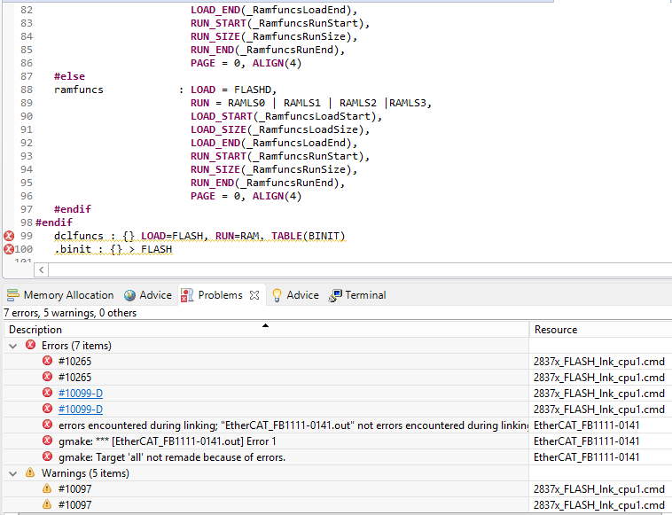
The cmd file is excluded from build in both RAM and FLASH configurations by the default ControlSuite Program and the HW_Init() function which is not causing any problem is the following:
//#############################################################################
//
// FILE: ethercat_slave_c28x_hal.c
//
// TITLE: C28x HAL level functions for EtherCAT slave controller (ESC)
//
//! \addtogroup C2k_EtherCAT_adapater_examples_list
//! <h1> PDI Interface test Example </h1>
//!
//! The functions in this file provide a HAL layer interface for EtherCAT slave
//! applications that can be built on C2k EtherCAT adapter board
//!
//! The HAL could be EMIF or SPI based depending on the PDI interface chosen
//! or configured for the C2k ET1100 EtherCAT adapater board
//!
//!-----------------------------------------------------------------------------
//! C28x Addressing vs. TwinCat3 software addresses for EMIF PDI
//! The C28x address used below is a WORD (16b) address for the ET1100 PDI
//! interface, while Beckhoff EtherCAT documentation and TwinCat3 software use
//! BYTE addresses. The USER RAM on the ET1100 starts at 0x1000 offset BYTE
//! address. Divide this by 2 to get the correct 16b word offset from EMIF2
//! start address
//!
//! EMIF PDI reads two bytes at a time from ET1100 address space, that is the
//! minimum data size thats readable by C28x CPU
//!------------------------------------------------------------------------------
//!------------------------------------------------------------------------------
//! C28x Addressing vs. TwinCat3 software addresses for SPI PDI
//! For the SPI PDI the addressing of ET1100 memory space is straight forward
//! The SPI PDI uses 8 bit character length for SPI reads/writes but the HAL API
//! is adjusted to read 16bits at a time to be consistent with the EMIF PDI.
//! Users can modify the SPI PDI to read/write one byte at a time from ET1100
//! address space. But since C28x data bus is 16 bit wide this example shows
//! 16bit SPI PDI reads/writes as well.
//!
//! SPI MISO pin read for error status on the last transaction is not supported
//! in this HAL
//! SPI MODE 3 is supported by this HAL
//! I0 and I1 byte reads on the MISO pin are ignored in this HAL
//!------------------------------------------------------------------------------
//! \b External \b Connections \n
//! Users can connect a PC running TWINCAT3 to the Ethercat Slave and view the
//! memory window of ET1100 for both registers and ET1100 RAM
//!
//! \b Watch \b Variables \n
//! - escRegs data structure is filled in with some ET1100 registers which can be
//! viewed in memory window if HAL Test is enabled.
//!
//!
////###########################################################################
// $TI Release: C2000 EtherCAT solutions support v1.00 $
// $Release Date: 07/2017 $
// $Copyright:
// Copyright (C) 2017 Texas Instruments Incorporated - http://www.ti.com/
//
// Redistribution and use in source and binary forms, with or without
// modification, are permitted provided that the following conditions
// are met:
//
// Redistributions of source code must retain the above copyright
// notice, this list of conditions and the following disclaimer.
//
// Redistributions in binary form must reproduce the above copyright
// notice, this list of conditions and the following disclaimer in the
// documentation and/or other materials provided with the
// distribution.
//
// Neither the name of Texas Instruments Incorporated nor the names of
// its contributors may be used to endorse or promote products derived
// from this software without specific prior written permission.
//
// THIS SOFTWARE IS PROVIDED BY THE COPYRIGHT HOLDERS AND CONTRIBUTORS
// "AS IS" AND ANY EXPRESS OR IMPLIED WARRANTIES, INCLUDING, BUT NOT
// LIMITED TO, THE IMPLIED WARRANTIES OF MERCHANTABILITY AND FITNESS FOR
// A PARTICULAR PURPOSE ARE DISCLAIMED. IN NO EVENT SHALL THE COPYRIGHT
// OWNER OR CONTRIBUTORS BE LIABLE FOR ANY DIRECT, INDIRECT, INCIDENTAL,
// SPECIAL, EXEMPLARY, OR CONSEQUENTIAL DAMAGES (INCLUDING, BUT NOT
// LIMITED TO, PROCUREMENT OF SUBSTITUTE GOODS OR SERVICES; LOSS OF USE,
// DATA, OR PROFITS; OR BUSINESS INTERRUPTION) HOWEVER CAUSED AND ON ANY
// THEORY OF LIABILITY, WHETHER IN CONTRACT, STRICT LIABILITY, OR TORT
// (INCLUDING NEGLIGENCE OR OTHERWISE) ARISING IN ANY WAY OUT OF THE USE
// OF THIS SOFTWARE, EVEN IF ADVISED OF THE POSSIBILITY OF SUCH DAMAGE.
// $
//#############################################################################
//
// Included Files
//
#include "F28x_Project.h" // Device Headerfile and Examples Include File
#include "F2837xD_spi.h"
#include "DCL.h"
#include "AdcSetup.h"
#include "Posspeed.h"
#include "ethercat_slave_c28x_hal.h"
//
// Defines
//
//#define ETHERCAT_STACK 1 //only use if EtherCAT slave stack is used
//
// Global Variables
//
int AdcaResult0, AdcbResult0, AdcaResult1, AdcbResult1, dc;
float analog1 = 0.0f;
DCL_PID pid1 = PID_DEFAULTS;
float rk1;
float yk1;
float lk1;
float uk1;
float Duty1;
DCL_PID pid2 = PID_DEFAULTS;
float rk2;
float yk2;
float lk2;
float uk2;
float Duty2;
//eqep
POSSPEED qep_posspeed=POSSPEED_DEFAULTS;
Uint16 int1cnt = 0;
Uint16 int2cnt = 0;
float desired_pos_high = 360.0;
float desired_pos_low = 0.0;
float desired_pos = 360.0;
long int raw_pos1, raw_pos2, raw_pos3;
long int angle_count1=0;
unsigned long int pos_init = 2147483647; //0x7fffffff
float gwnia1, gwnia2, gwnia3;
float ngwnia1, ngwnia2, ngwnia3;
int dir = 0;
//Pointer to the ESC memory, initialized in the ESC_initHW()
//used only for the ASYNC16 (EMIF1 or EMIF2) PDI
//uint16_t *pEsc;
#ifdef PDI_HAL_TEST
//Debug array to log esc registers, used only for PDI HAL TEST
esc_et1100_regs_t escRegs[ESC_DEBUG_REGS_LENGTH];
#endif
#ifdef INTERFACE_SPI
// SPI Variables
volatile uint16_t SPI_RxData[16]; // Receive data buffer
volatile uint16_t SPI_XmitInProgress;
#endif
//
//HAL level functions
//
#ifndef __cplusplus
#ifdef INTERFACE_SPI
#pragma CODE_SECTION(ESC_readSPI, ".TI.ramfunc");
#pragma CODE_SECTION(ESC_writeSPI, ".TI.ramfunc");
#endif
#pragma CODE_SECTION(ESC_timerIncPerMilliSec, ".TI.ramfunc");
#pragma CODE_SECTION(ESC_getTimer, ".TI.ramfunc");
#endif
/***********************************************************************************/
//Set the GPyDAT register bit for the specified pin.
uint32_t ESC_getTimer(void)
{
//C28x timer is decrements from 0xFFFFFFFF while the stack understands it as of
//increment type.
return ~ ((uint32_t)(CpuTimer0Regs.TIM.all));
}
/***********************************************************************************/
void ESC_clearTimer(void)
{
CpuTimer0Regs.TIM.all = 0;
}
/***********************************************************************************/
uint32_t ESC_timerIncPerMilliSec(void)
{
return (uint32_t) 200000UL; //at 200MHz
}
/***********************************************************************************/
//
// SPI HAL functions for EtherCAT slave stack
//
//SPI peripehral register pointer, will be initialized depending on the SPI chosen as per
// build configurations
volatile struct SPI_REGS *SpixRegs;
/*****************************************************************************************
* @fn ESC_readSPI
* @brief function reads up to 12 bytes of data
*
* @param
* offset_addr - ESC address from which data has to be read
* numbytes - number of bytes to be read, limited to 12 at a time by the caller
* buffer - pointer to the buffer where read data has to be copied to
* - if a NULL is passed then data is copied to SPI_RxData global array
*
* @return - None
****************************************************************************************/
void ESC_readSPI(uint16_t offset_addr,uint16_t numbytes, uint16_t* buffer)
{
uint16_t i,cmd, readval, numwords = 0, j;
uint16_t *buf = (uint16_t *)0;
uint16_t readphase[16];
if(((void *)buffer) == NULL)
{
buf = (uint16_t *)&SPI_RxData[0];
}
else
{
buf = buffer;
}
// Construct Address cmd bytes into 16-bit words for SPI xmission,
// SPI xmits MSBit 1st, so must swap bytes in this 16b word for transmission
// Byte order of READ cmd sequence:
// Byte 0: A[12:5]
// Byte 1: A[4:0], 110b (110b is 3-byte cmd extension)
// Byte 2: A[15:13], CMD[2:0], 00b (011b is READ w/ WS)
// Byte 3: FFh (Wait State)
//cmd = offset_addr & 0x1f
cmd =(offset_addr & 0x1FE0)<<3; // offset_addr[12:5] is 1st address phase byte, shift to upper byte
cmd |= (((offset_addr & 0x1F) << 3) | ESC_ETHERCAT_3BYTEADDR);
readphase[0] = cmd;
numwords++;
readphase[1] = (offset_addr & 0xE000) | (ESC_ETHERCAT_READ_WAIT <<10) | ESC_ETHERCAT_WAIT;
numwords++;
for(i=2, j = 0; j<numbytes ; i++){
readphase[i] = (uint16_t) ESC_ETHERCAT_CONTINUE;
numwords++;
j++;
j++;
}
readphase[--i] |= (ESC_ETHERCAT_RDTERMINATE); // set last byte as 0xFF
for(i = 0;i < numwords;i++){
SpixRegs->SPITXBUF = readphase[i] & (0xFF00);
SpixRegs->SPITXBUF = ((readphase[i] & (0xFF)) << 8);
}
SPI_XmitInProgress=1;
DELAY_US(10);
j = numbytes;
while(SpixRegs->SPIFFRX.bit.RXFFST < (numwords))
{
asm(" NOP"); //need 12ns delay
asm(" NOP");
asm(" NOP");
};
while(SpixRegs->SPIFFRX.bit.RXFFST != (numbytes))
{
////ignore first two words (4 bytes)
readval = SpixRegs->SPIRXBUF; //ignore
}
for(i=0;((SpixRegs->SPIFFRX.bit.RXFFST != 0));i++)
{
readval = (SpixRegs->SPIRXBUF) & 0xFF;
buf[i]= (readval & 0xFF);
readval = (SpixRegs->SPIRXBUF) & 0xFF;
buf[i] |= ((readval & 0xFF) << 8);
}
DELAY_US(5);
SpixRegs->SPIFFTX.bit.TXFIFO=0; // Reset Tx FIFO
SpixRegs->SPIFFRX.bit.RXFIFORESET = 0; //reset the FIFO pointer
DELAY_US(2);
SpixRegs->SPIFFTX.bit.TXFIFO=1; // Reenable Tx FIFO
SpixRegs->SPIFFRX.bit.RXFIFORESET = 1; //reenable the FIFO operation
SPI_XmitInProgress=0;
}
#define FIFO_LENGTH 12
/*****************************************************************************************
* @fn ESC_writeSPI
* @brief function writes up to 12 bytes of data
*
* @param
* offset_addr - ESC address to which data has to written to
* numbytes - number of bytes to be written to, limited to 12 at a time by the caller
* wrdata - pointer to the buffer from where data has to be written to ESC
*
*
* @return - none
****************************************************************************************/
void ESC_writeSPI(uint16_t offset_addr,uint16_t *wrdata, uint16_t numbytes)
{
uint16_t i, j,cmd, numwords = 0;
uint16_t wptr = 0;
uint16_t writephase[2];
// Construct Address cmd bytes into 16-bit words for SPI xmission,
// SPI xmits MSBit 1st, so must swap bytes in this 16b word for transmission
// Byte order of READ cmd sequence:
// Byte 0: A[12:5]
// Byte 1: A[4:0], 110b (110b is 3-byte cmd extension)
// Byte 2: A[15:13], CMD[2:0], 00b (110b is 3-byte cmd extension)
// Byte 3: Afirst byte of data
//cmd = offset_addr & 0x1f
cmd =(offset_addr & 0x1FE0)<<3; // offset_addr[12:5] is 1st address phase byte, shift to upper byte
cmd |= (((offset_addr & 0x1F) << 3) | ESC_ETHERCAT_3BYTEADDR);
writephase[0] = cmd;
numwords++;
cmd = 0x0000;
cmd = (((offset_addr & 0xE000) | (ESC_ETHERCAT_WRITE <<10))) ;
cmd |= (wrdata[wptr] & 0x00FF);
writephase[1] = cmd;
numwords++;
i = 0;
{
SpixRegs->SPITXBUF = writephase[i] & (0xFF00);
SpixRegs->SPITXBUF = ((writephase[i++] & (0xFF)) << 8);
SpixRegs->SPITXBUF = writephase[i] & (0xFF00);
SpixRegs->SPITXBUF = ((writephase[i] & (0xFF)) << 8);
}
wptr=0;
for(j = 1; j < (numbytes-1) ; j+=2)
{
SpixRegs->SPITXBUF = ((wrdata[wptr]) & 0xFF00);
SpixRegs->SPITXBUF= (((wrdata[++wptr]) & 0x00FF) << 8);
numwords++;
}
if(j == (numbytes-1))
{
SpixRegs->SPITXBUF = ((wrdata[wptr]) & 0xFF00);
numwords++;
}
SPI_XmitInProgress=1;
while(SpixRegs->SPIFFTX.bit.TXFFST != 0)
{
DELAY_US(2);
};
SpixRegs->SPIFFTX.bit.TXFIFO=0; // Reset Tx FIFO
SpixRegs->SPIFFRX.bit.RXFIFORESET = 0; //reset the FIFO pointer
DELAY_US(2);
SpixRegs->SPIFFTX.bit.TXFIFO=1; // Reset Tx FIFO
SpixRegs->SPIFFRX.bit.RXFIFORESET = 1; //reenable the FIFO operation
SPI_XmitInProgress=0;
}
/***********************************************************************************/
uint16_t ESC_readWordNonISR(uint16_t offset_addr)
{
uint16_t data;
DINT;
ESC_readSPI(offset_addr, 2, &data);
EINT;
return data;
}
/***********************************************************************************/
uint16_t ESC_readWordISR(uint16_t offset_addr)
{
ESC_readSPI(offset_addr, 2, 0);
return (SPI_RxData[0]);
}
/***********************************************************************************/
uint32_t ESC_readDWordNonISR(uint16_t offset_addr)
{
uint32_t dword;
DINT;
ESC_readSPI(offset_addr, 4, (uint16_t *)&dword);
EINT;
return dword;
}
/***********************************************************************************/
uint32_t ESC_readDWordISR(uint16_t offset_addr)
{
uint32_t dword;
ESC_readSPI(offset_addr, 4, (uint16_t *)&dword);
return dword;
}
/***********************************************************************************/
void ESC_readBlockISR(uint16_t* pData, uint16_t offset_addr,uint16_t numbytes)
{
uint16_t i = 0, current_bytes = 0, last_byte = 0;
if(numbytes & 0x1)
{
current_bytes = (numbytes - 0x1); // even align
}
else
{
current_bytes = numbytes;
}
while(current_bytes > 0) // input is actually in bytes
{
if( current_bytes >= FIFO_LENGTH)
{
ESC_readSPI(offset_addr, FIFO_LENGTH, (uint16_t *) &pData[i]);
current_bytes -= FIFO_LENGTH;
i+= FIFO_LENGTH/2; // data is in 16 bits
offset_addr += FIFO_LENGTH;
}
else
{
ESC_readSPI(offset_addr, current_bytes, (uint16_t *) &pData[i]);
offset_addr += current_bytes;
i+= current_bytes/2;
current_bytes = 0;
}
}
if(numbytes & 0x1)
{
last_byte = ESC_readWordISR(offset_addr);
pData[i] = pData[i] & 0xFF00;
pData[i] |= last_byte;
}
}
/***********************************************************************************/
void ESC_readBlockNonISR(uint16_t* pData, uint16_t offset_addr,uint16_t numbytes)
{
DINT;
ESC_readBlockISR(pData, offset_addr,numbytes);
EINT;
}
/***********************************************************************************/
void ESC_writeWordNonISR(uint16_t wrdata, uint16_t offset_addr)
{
DINT;
ESC_writeSPI(offset_addr, &wrdata, 0x02);
EINT;
}
/***********************************************************************************/
void ESC_writeWordISR(uint16_t wrdata, uint16_t offset_addr)
{
ESC_writeSPI(offset_addr, &wrdata, 0x02);
}
/***********************************************************************************/
void ESC_writeDWordNonISR(uint32_t wrdata, uint16_t offset_addr)
{
DINT;
ESC_writeSPI(offset_addr, (uint16_t *)&wrdata, 0x04);
EINT;
}
/***********************************************************************************/
void ESC_writeDWordISR(uint32_t wrdata, uint16_t offset_addr)
{
ESC_writeSPI(offset_addr, (uint16_t *)&wrdata, 0x04);
}
/***********************************************************************************/
void ESC_writeBlockISR(uint16_t* pData, uint16_t offset_addr,uint16_t numbytes)
{
uint16_t i = 0, current_bytes = 0;
if(numbytes & 0x1)
{
current_bytes = (numbytes - 0x1); // even align
}
else
{
current_bytes = (numbytes);
}
while(current_bytes > 0) // input is actually in bytes
{
if( current_bytes >= FIFO_LENGTH)
{
ESC_writeSPI(offset_addr, (uint16_t *) &pData[i], FIFO_LENGTH);
current_bytes -= FIFO_LENGTH;
i+= FIFO_LENGTH/2; // data is in 16 bits
offset_addr += FIFO_LENGTH;
}
else
{
ESC_writeSPI(offset_addr, (uint16_t *) &pData[i], current_bytes);
offset_addr += current_bytes;
i+= current_bytes/2;
current_bytes = 0;
}
}
if(numbytes & 0x1)
{
//now send the last byte with extra alignment bytes
// note that we read the adjacent byte and write it back
ESC_readSPI(offset_addr, 2, &i);
i &= 0xFF00;
i |= (pData[((numbytes-1) >> 1)]) & 0xFF; //pData is 16bit pointer
ESC_writeSPI(offset_addr, &i, 2);
}
}
/***********************************************************************************/
void ESC_writeBlockNonISR(uint16_t* pData, uint16_t offset_addr,uint16_t numbytes)
{
DINT;
ESC_writeBlockISR(pData, offset_addr,numbytes);
EINT;
}
//-----------------------------------------------------------------------------------
// Function to initialize SPI port
//-----------------------------------------------------------------------------------
void ESC_initSPIFIFO(void)
{
uint16_t m;
EALLOW;
// FIFO configuration
SpixRegs->SPIFFCT.all=0x0; // place SPI in reset
for(m=0;m<3;m++);
SpixRegs->SPIFFRX.all=0x2040; // RX FIFO enabled, clear FIFO int
SpixRegs->SPIFFRX.bit.RXFFIL = 16; // Set RX FIFO level
SpixRegs->SPIFFTX.all=0xE040; // FIFOs enabled, TX FIFO released,
// SPI configuration
SpixRegs->SPIFFTX.bit.TXFFIL = 16; // Set TX FIFO level
SpixRegs->SPICCR.bit.SPICHAR = 0x7;//0xF; // Character Length = 8
SpixRegs->SPICCR.bit.CLKPOLARITY = 1; // Rising edge
SpixRegs->SPICCR.bit.HS_MODE = 0; // Not high speed mode
SpixRegs->SPICTL.bit.SPIINTENA = 1; // Enabled
SpixRegs->SPICTL.bit.TALK = 1; //
SpixRegs->SPICTL.bit.MASTER_SLAVE = 1; // Master mode
SpixRegs->SPICTL.bit.CLK_PHASE = 0; // Add 1/2-cycle delay of Clk wrt SPISTEA
SpixRegs->SPICTL.bit.OVERRUNINTENA = 1; // Overrun Interrupt enabled
SpixRegs->SPISTS.all=0x0000; // Clear Status bits (TxBufFull,INT, Overrun)
// SpixRegs->SPIBRR.all = 0x63; // LSPCLK/100
ClkCfgRegs.LOSPCP.all = 0x1; // 0 = sysclk/1 = 200M; 1 = sysclk/2 = 100M
SpixRegs->SPIBRR.all=0x004; // Baud Rate = LSPCLK / (SPIBRR+1) [LSPCLK=SysClk/4 by default=50M]
SpixRegs->SPIFFCT.all=0x00;
SpixRegs->SPIPRI.all=0x0020; // Stop after transaction complete on EmuStop
SpixRegs->SPIFFTX.bit.TXFFIENA = 0; // Disable TXFF INT
SpixRegs->SPIFFRX.bit.RXFFIENA = 0; // disable RXFF INT
SpixRegs->SPICCR.bit.SPISWRESET=1; // Enable SPI
EDIS;
}
//-----------------------------------------------------------------------------------
// Function to initialize GPIOs for SPIB port
// GPIO64, GPIO65, GPIO66, GPIO63
// Not used in TMDSECATCNCD379D kit
//-----------------------------------------------------------------------------------
void ESC_initSPIBGpio(void)
{
EALLOW;
// Enable pull-ups on SPISIMO/SPISOMI/SPICLK/SPISTE pins
GpioCtrlRegs.GPCPUD.all &= 0xFFFFFFF8;
GpioCtrlRegs.GPBPUD.all &= 0xFFFFFFFE;
// Enable SPISIMO/SPISOMI/SPICLK pins
GpioCtrlRegs.GPCGMUX1.bit.GPIO64 = 0x3;
GpioCtrlRegs.GPCMUX1.bit.GPIO64 = 0x3;
GpioCtrlRegs.GPCGMUX1.bit.GPIO65 = 0x3;
GpioCtrlRegs.GPCMUX1.bit.GPIO65 = 0x3;
GpioCtrlRegs.GPCGMUX1.bit.GPIO66 = 0x3;
GpioCtrlRegs.GPCMUX1.bit.GPIO66 = 0x3;
GpioCtrlRegs.GPBGMUX2.bit.GPIO63 = 0x3;
GpioCtrlRegs.GPBMUX2.bit.GPIO63 = 0x3;
// Enable SPISIMO/SPISOMI/SPICLK pins as async
GpioCtrlRegs.GPCQSEL1.all |= 0xF;
GpioCtrlRegs.GPBQSEL2.bit.GPIO63 = 0x3;
EDIS;
}
//-----------------------------------------------------------------------------------
// Function to initialize GPIOs for *** port
// GPIO122, GPIO123, GPIO124, GPIO125
// Function used in TMDSECATCNCD379D kit
//-----------------------------------------------------------------------------------
void ESC_initSPICGpio(void)
{
EALLOW;
// new control card with HD connector
// Enable pull-ups on SPISIMO/SPISOMI/SPICLK/SPISTE pins
//GPIO122,123,124,125
GpioCtrlRegs.GPDPUD.all &= 0xC3FFFFFF;
// Enable SPISIMO/SPISOMI/SPICLK pins
GpioCtrlRegs.GPDGMUX2.bit.GPIO122 = 0x1;
GpioCtrlRegs.GPDGMUX2.bit.GPIO123 = 0x1;
GpioCtrlRegs.GPDGMUX2.bit.GPIO124 = 0x1;
GpioCtrlRegs.GPDGMUX2.bit.GPIO125 = 0x1;
GpioCtrlRegs.GPDMUX2.bit.GPIO122 = 0x2;
GpioCtrlRegs.GPDMUX2.bit.GPIO123 = 0x2;
GpioCtrlRegs.GPDMUX2.bit.GPIO124 = 0x2;
GpioCtrlRegs.GPDMUX2.bit.GPIO125 = 0x2;
// Enable SPISIMO/SPISOMI/SPICLK pins as async
GpioCtrlRegs.GPDQSEL2.all |= 0x03F00000;
EDIS;
}
//-----------------------------------------------------------------------------------
// Function to initialize GPIOs for SPIÁ port
// GPIO58(SIMOA), GPIO59(SOMIA), GPIO60(CLKA), GPIO61(SELA)
// GPIO16, GPIO17, GPIO18, GPIO19 (commented out)
// Not used in TMDSECATCNCD379D kit
//-----------------------------------------------------------------------------------
void ESC_initSPIAGpio(void)
{
EALLOW;
/* Enable internal pull-up for the selected pins */
// Pull-ups can be enabled or disabled by the user.
// This will enable the pullups for the specified pins. Enable pull-ups on SPISIMO/SPISOMI/SPICLK/SPISTE pins
GpioCtrlRegs.GPBPUD.bit.GPIO58 = 0; // Enable pull-up on GPIO58 (SPISIMO-A)
GpioCtrlRegs.GPBPUD.bit.GPIO59 = 0; // Enable pull-up on GPIO59 (SPISOMI-A)
GpioCtrlRegs.GPBPUD.bit.GPIO60 = 0; // Enable pull-up on GPIO60 (SPICLK-A)
GpioCtrlRegs.GPBPUD.bit.GPIO61 = 0; // Enable pull-up on GPIO61 (SPISTE-A)
/* Set qualification for selected pins to asynch only */
// This will select asynch (no qualification) for the selected pins.
GpioCtrlRegs.GPBQSEL2.bit.GPIO58 = 3; // Asynch input GPIO58 (SPISIMO-A)
GpioCtrlRegs.GPBQSEL2.bit.GPIO59 = 3; // Asynch input GPIO59 (SPISOMI-A)
GpioCtrlRegs.GPBQSEL2.bit.GPIO60 = 3; // Asynch input GPIO60 (SPICLK-A)
GpioCtrlRegs.GPBQSEL2.bit.GPIO61 = 3; // Asynch input GPIO61 (SPISTE-A)
//Configure SPI-A pins using GPIO regs
// This specifies which of the possible GPIO pins will be SPI functional pins.
//G-Mux
GpioCtrlRegs.GPBGMUX2.bit.GPIO58 = 3; // Enable (SPISIMO-A)
GpioCtrlRegs.GPBGMUX2.bit.GPIO59 = 3; // Enable (SPISOMI-A)
GpioCtrlRegs.GPBGMUX2.bit.GPIO60 = 3; // Enable (SPISCLK-A)
GpioCtrlRegs.GPBGMUX2.bit.GPIO61 = 3; // Enable (SPISTE-A)
//Mux
GpioCtrlRegs.GPBMUX2.bit.GPIO58 = 3; // Enable (SPISIMO-A)
GpioCtrlRegs.GPBMUX2.bit.GPIO59 = 3; // Enable (SPISOMI-A)
GpioCtrlRegs.GPBMUX2.bit.GPIO60 = 3; // Enable (SPISCLK-A)
GpioCtrlRegs.GPBMUX2.bit.GPIO61 = 3; // Enable (SPISTE-A)
EDIS;
}
/*EALLOW; (OLDER CONFIGURATION from TI for SPI-A and GPIOs 16,17,18,19)
// Enable pull-ups on SPISIMO/SPISOMI/SPICLK/SPISTE pins
GpioCtrlRegs.GPAPUD.all &= 0xFFF0FFFF;
// Enable SPISIMO/SPISOMI/SPICLK pins
GpioCtrlRegs.GPAMUX2.all |= 0x00000055;
// Enable SPISIMO/SPISOMI/SPICLK pins as async
GpioCtrlRegs.GPAQSEL2.all |= 0x0000003F;
EDIS;
}*/
/***********************************************************************************/
void ESC_releaseET1100Reset(void)
{
GPIO_SetupPinMux(ESC_RESET_ET1100_GPIO, GPIO_MUX_CPU1, 0);
GPIO_WritePin(ESC_RESET_ET1100_GPIO, 1); //release reset
}
/***********************************************************************************/
void ESC_holdET1100InReset(void)
{
GPIO_SetupPinMux(ESC_RESET_ET1100_GPIO, GPIO_MUX_CPU1, 0);
GPIO_WritePin(ESC_RESET_ET1100_GPIO, 0); //hold in reset
}
/***********************************************************************************/
void ESC_configureLatch0GPIO(void)
{
//This function configures SYNC0 GPIO as LATCH OUTPUT (Input to ESC)
GPIO_SetupPinOptions(ESC_SYNC0_GPIO, GPIO_OUTPUT, GPIO_PULLUP);
GPIO_SetupPinMux(ESC_SYNC0_GPIO, GPIO_MUX_CPU1, 0);
}
/***********************************************************************************/
void ESC_configureLatch1GPIO(void)
{
//This function configures SYNC1 GPIO as LATCH OUTPUT
GPIO_SetupPinOptions(ESC_SYNC1_GPIO, GPIO_OUTPUT, GPIO_PULLUP);
GPIO_SetupPinMux(ESC_SYNC1_GPIO, GPIO_MUX_CPU1, 0);
}
//-----------------------------------------------------------------------------------
// ISR to handle PDI ISR
//-----------------------------------------------------------------------------------
interrupt void ESC_applicationLayerISR()
{
//call the slave stack ISR routine
#ifdef ETHERCAT_STACK
PDI_Isr();
#endif
PieCtrlRegs.PIEACK.all |= 0x01; // Issue PIE ack
}
//-----------------------------------------------------------------------------------
// ISR to handle SYNC0 ISR
//-----------------------------------------------------------------------------------
interrupt void ESC_applicationSync0ISR()
{
#ifdef ETHERCAT_STACK
Sync0_Isr();
#endif
//XINT5, PIE 12.INT3
PieCtrlRegs.PIEACK.bit.ACK12 = 1;
}
//-----------------------------------------------------------------------------------
// ISR to handle SYNC1 ISR
//-----------------------------------------------------------------------------------
interrupt void ESC_applicationSync1ISR()
{
#ifdef ETHERCAT_STACK
Sync1_Isr();
#endif
//XINT4, PIE 12.INT2
PieCtrlRegs.PIEACK.bit.ACK12 = 1;
}
//-----------------------------------------------------------------------------------
// Function to enable debug of SYNC0 signal on ControlCard configurations
//-----------------------------------------------------------------------------------
void ESC_enableSync0DebugOnCCARD(void)
{
//for debug of SYNC0 line.- the below code connects GPIO2 to the SYNC0
//internally because on the HW board we cannot put a scope on SYNC0 on HighRose connector
//Connect SYNC0 (GPIO86) is INPUT1 for
EALLOW;
InputXbarRegs.INPUT1SELECT = ESC_SYNC0_GPIO; //input1 is tied to GPIO113
OutputXbarRegs.OUTPUT1MUX0TO15CFG.bit.MUX1 = 0x1; //INPUTXBAR1 to OUTPUTXBAR1
OutputXbarRegs.OUTPUT1MUXENABLE.bit.MUX1 = 0x1;
GpioCtrlRegs.GPAGMUX1.bit.GPIO2 = 0x01; //GPIO2 to OUTPUTXBAR1
GpioCtrlRegs.GPAMUX1.bit.GPIO2 = 0x01;
EDIS;
}
//-----------------------------------------------------------------------------------
// Function to configure SYNC0 signal on ControlCard configurations
//-----------------------------------------------------------------------------------
void ESC_configureSync0GPIO(void)
{
GPIO_SetupPinOptions(ESC_SYNC0_GPIO, GPIO_INPUT, GPIO_PULLUP| GPIO_ASYNC);
GPIO_SetupPinMux(ESC_SYNC0_GPIO, GPIO_MUX_CPU1, 0);
EALLOW;
InputXbarRegs.INPUT14SELECT = ESC_SYNC0_GPIO; //input14 is tied to XINT5
PieVectTable.XINT5_INT = &ESC_applicationSync0ISR;
XintRegs.XINT5CR.bit.POLARITY = 1; // Falling edge interrupt
XintRegs.XINT5CR.bit.ENABLE = 1;
PieCtrlRegs.PIEIER12.bit.INTx3 = 1; // Enable Group 12, INT3 (XINT5)
IER |= 0x0800;
EDIS; // This is needed to disable write to EALLOW protected registers
ESC_enableSync0DebugOnCCARD();
}
//-----------------------------------------------------------------------------------
// Function to enable debug of SYNC0 signal on ControlCard configurations
//-----------------------------------------------------------------------------------
void ESC_enableSync1DebugOnCCARD(void)
{
//for debug of SYNC1 line.- the below code connects GPIO3 to the SYNC1
//internally because on the HW board we cannot put a scope on SYNC1 on HighRose connector
//Connect SYNC1 is INPUT1 for
EALLOW;
InputXbarRegs.INPUT2SELECT = ESC_SYNC1_GPIO; //input2 is tied to SYNC1
OutputXbarRegs.OUTPUT2MUX0TO15CFG.bit.MUX3 = 0x1; //INPUTXBAR2 to OUTPUTXBAR2
OutputXbarRegs.OUTPUT2MUXENABLE.bit.MUX3 = 0x1;
GpioCtrlRegs.GPAGMUX1.bit.GPIO3 = 0x01; //GPIO3 to OUTPUTXBAR2
GpioCtrlRegs.GPAMUX1.bit.GPIO3 = 0x01;
EDIS;
}
//-----------------------------------------------------------------------------------
// Function to configure SYNC1 signal on ControlCard configurations
//-----------------------------------------------------------------------------------
void ESC_configureSync1GPIO(void)
{
GPIO_SetupPinOptions(ESC_SYNC1_GPIO, GPIO_INPUT, GPIO_PULLUP| GPIO_ASYNC);
GPIO_SetupPinMux(ESC_SYNC1_GPIO, GPIO_MUX_CPU1, 0);
EALLOW;
InputXbarRegs.INPUT13SELECT = ESC_SYNC1_GPIO; //input13 is tied to XINT4
PieVectTable.XINT4_INT = &ESC_applicationSync1ISR;
XintRegs.XINT4CR.bit.POLARITY = 1; // Falling edge interrupt
XintRegs.XINT4CR.bit.ENABLE = 1;
PieCtrlRegs.PIEIER12.bit.INTx2 = 1; // Enable Group 12, INT2 (XINT4)
IER |= 0x0800;
EDIS; // This is needed to disable write to EALLOW protected registers
ESC_enableSync1DebugOnCCARD();
}
/***********************************************************************************/
void ESC_resetET1100(void)
{
GPIO_SetupPinMux(ESC_RESET_ET1100_GPIO, GPIO_MUX_CPU1, 0);
GPIO_WritePin(ESC_RESET_ET1100_GPIO, 0); //hold reset low
DELAY_US(500*1000);
GPIO_WritePin(ESC_RESET_ET1100_GPIO, 1); //release reset
DELAY_US(500*1000);
}
/***********************************************************************************/
uint16_t ESC_ET1100EEPROMLoadedCheck(void)
{
uint16_t ii = 0;
GPIO_SetupPinMux(ESC_EEPROM_LOADED_GPIO, GPIO_MUX_CPU1, 0);
while(!GPIO_ReadPin(ESC_EEPROM_LOADED_GPIO))
{
DELAY_US(500*1000);
ii++;
if(ii > 10)
break;
}
if(ii > 10)
return 0;
else
return 1;
}
/***********************************************************************************/
void ESC_passFailSignalSetup(void)
{
// Note:- This function is not called when EMIF1 is used because there
// is conflict with GPIO31 and GPIO34 with EMIF1 signals and LEDs
// so with LAUNCHXL2.0 , user will only know if there is an error
// Both LEDs (GPIO31 and GPIO34 HIGH or LOW always means no error on
// Launchpad XL 2.0)
GPIO_SetupPinMux(34, GPIO_MUX_CPU1, 0);
GPIO_SetupPinMux(31, GPIO_MUX_CPU1, 0);
GPIO_SetupPinOptions(34, 1, GPIO_OPENDRAIN | GPIO_PULLUP);
GPIO_SetupPinOptions(31, 1, GPIO_OPENDRAIN | GPIO_PULLUP);
//GPIO34 and GPIO31 at HIGH - means NO ERROR
//keep GPIO31 and GPIO34 LOW for PASS - by default
GpioDataRegs.GPADAT.bit.GPIO31 = 1;
GpioDataRegs.GPBDAT.bit.GPIO34 = 1;
}
/***********************************************************************************/
void ESC_signalFail(void)
{
//Toggle GPIO34 and GPIO31 for fail
GpioDataRegs.GPBTOGGLE.bit.GPIO34 = 1;
GpioDataRegs.GPATOGGLE.bit.GPIO31 = 1;
DELAY_US(10 * 1000);
}
/***********************************************************************************/
void ESC_signalPass(void)
{
//keep GPIO31 and GPIO34 LOW for PASS
GpioDataRegs.GPADAT.bit.GPIO31 = 1;
GpioDataRegs.GPBDAT.bit.GPIO34 = 1;
DELAY_US(500 * 1000);
}
//-----------------------------------------------------------------------------------
// ISR to handle EPWM1 ISR
// prdTick - EPWM1 Interrupts once every 4 QCLK counts (one period)
//-----------------------------------------------------------------------------------
interrupt void epwm1_isr(void)
{
if (int1cnt == 2) //10khz control loop frequency
{
EALLOW;
//Uncomment the following lines to enable reading the values of the 3rd encoder
//-----------------------------------------------------------------------------
// // 3rd Encoder Read
// // Read raw values of eQEPs
// qep_posspeed.calc(&qep_posspeed);
//
// //Read raw position eQEP3
// if ((unsigned long int) qep_posspeed.raw_pos3 > pos_init)
// raw_pos3 = (unsigned long int) qep_posspeed.raw_pos3 - pos_init;
// else
// raw_pos3 = -(pos_init - (unsigned long int) qep_posspeed.raw_pos3);
// gwnia3 = 360.0f * (raw_pos3 * 8.0f * 26.0f)
// / (2000.0f * 343.0f * 48.0f); //2000 lines
//-----------------------------------------------------------------------------
// Control Motor 1 Knee (BLDC)
// 1st Encoder Read
// Read raw values of eQEPs
qep_posspeed.calc(&qep_posspeed);
//Read raw position eQEP1
if ((unsigned long int) qep_posspeed.raw_pos1 > pos_init)
raw_pos1 = (unsigned long int) qep_posspeed.raw_pos1 - pos_init;
else
raw_pos1 = -(pos_init - (unsigned long int) qep_posspeed.raw_pos1);
angle_count1=raw_pos1;
//Translate raw value to degrees
gwnia1 = 360.0f * (raw_pos1 * 8.0f * 26.0f)/(2000.0f * 343.0f * 48.0f);
//Normalize value of gwnia1
ngwnia1 = (gwnia1 * 1.0f) / 360.0f;
// Run PID controller
uk1 = DCL_runPID_C4(&pid1, rk1, ngwnia1, lk1);
// Set direction
if (uk1 >= 0.0f)
GPIO_WritePin(DIR1_GPIO, 0);
else
{
GPIO_WritePin(DIR1_GPIO, 1);
uk1 = -uk1;
}
// Update PWM duty cycle
//EPwm1Regs.CMPA.bit.CMPA = (1.0f - uk1) * SP;
EPwm1Regs.CMPA.bit.CMPA = (1.0f-0.01*LED_Frequency) * SP;
int1cnt = 0;
}
int1cnt++;
EDIS;
// Clear INT flag for this timer
EPwm1Regs.ETCLR.bit.INT = 1;
//
// Acknowledge this __interrupt to receive more __interrupts from group 3
//
PieCtrlRegs.PIEACK.all = PIEACK_GROUP3;
}
//-----------------------------------------------------------------------------------
// ISR to handle EPWM2 ISR
// prdTick - EPWM2 Interrupts once every 4 QCLK counts (one period)
//-----------------------------------------------------------------------------------
interrupt void epwm2_isr(void)
{
if (int2cnt == 2) //10khz control loop frequency
{
EALLOW;
// Control Motor 2 Hip (Brushed DC)
// Read raw values of eQEPs
qep_posspeed.calc(&qep_posspeed);
if ((unsigned long int) qep_posspeed.raw_pos2 > pos_init)
raw_pos2 = (unsigned long int) qep_posspeed.raw_pos2 - pos_init;
else
raw_pos2 = -(pos_init - (unsigned long int) qep_posspeed.raw_pos2);
//Translate raw value to degrees
gwnia2 = 360.0f * (raw_pos2 * 12.0f * 26.0f)/(2000.0f * 637.0f * 48.0f);
//Normalize value of gwnia2
ngwnia2 = (gwnia2 * 1.0f) / 360.0f;
// Run PID controller
uk2 = DCL_runPID_C4(&pid2, rk2, ngwnia2, lk2);
// Set direction
if (uk2 >= 0.0f)
GPIO_WritePin(DIR2_GPIO, 0);
else
{
GPIO_WritePin(DIR2_GPIO, 1);
uk2 = -uk2;
}
// Update PWM duty cycle
EPwm2Regs.CMPA.bit.CMPA = (1.0f - uk2) * SP;
// Reset interrupt counter
int2cnt = 0;
}
int2cnt++;
EDIS;
// Clear INT flag for this timer
EPwm2Regs.ETCLR.bit.INT = 1;
//
// Acknowledge this __interrupt to receive more __interrupts from group 3
//
PieCtrlRegs.PIEACK.all = PIEACK_GROUP3;
}
//-----------------------------------------------------------------------------------
// Function to handle ADC Signals
//-----------------------------------------------------------------------------------
void ReadAnalog(void)
{
//
//convert, wait for completion, and store results
//start conversions immediately via software, ADCA
//
AdcaRegs.ADCSOCFRC1.all = 0x0003; //SOC0 and SOC1
//
//start conversions immediately via software, ADCB
//
AdcbRegs.ADCSOCFRC1.all = 0x0003; //SOC0 and SOC1
//
//wait for ADCA to complete, then acknowledge flag
//
while (AdcaRegs.ADCINTFLG.bit.ADCINT1 == 0)
;
AdcaRegs.ADCINTFLGCLR.bit.ADCINT1 = 1;
//
//wait for ADCB to complete, then acknowledge flag
//
while (AdcbRegs.ADCINTFLG.bit.ADCINT1 == 0)
;
AdcbRegs.ADCINTFLGCLR.bit.ADCINT1 = 1;
//
//store results
//
AdcaResult0 = AdcaResultRegs.ADCRESULT0;
AdcaResult1 = AdcaResultRegs.ADCRESULT1;
AdcbResult0 = AdcbResultRegs.ADCRESULT0;
AdcbResult1 = AdcbResultRegs.ADCRESULT1;
}
/***********************************************************************************/
void ESC_initHW(void)
{
#ifdef FLASH
// Copy time critical code and Flash setup code to RAM
// The RamfuncsLoadStart, RamfuncsLoadEnd, and RamfuncsRunStart
// symbols are created by the linker. Refer to the linker files.
memcpy(&RamfuncsRunStart, &RamfuncsLoadStart, (uint32_t)&RamfuncsLoadSize);
#endif
InitSysCtrl();
// Only used if running from FLASH
// Note that the variable FLASH is defined by the compiler
#ifdef FLASH
// Call Flash Initialization to setup flash waitstates
// This function must reside in RAM
InitFlash(); // Call the flash wrapper init function
#endif //(FLASH)
//
// enable PWM1, PWM2 and PWM3
//
CpuSysRegs.PCLKCR2.bit.EPWM1 = 1;
CpuSysRegs.PCLKCR2.bit.EPWM2 = 1;
//
// Clear all __interrupts and initialize PIE vector table:
// Disable CPU __interrupts
//
DINT;
// Initialize the PIE control registers to their default state.
// The default state is all PIE interrupts disabled and flags
// are cleared.
// This function is found in the F2837xD_PieCtrl.c file.
InitPieCtrl();
// Disable CPU interrupts and clear all CPU interrupt flags:
EALLOW;
IER = 0x0000;
IFR = 0x0000;
EDIS;
// Initialize the PIE vector table with pointers to the shell Interrupt
// GService Routines (ISR).
// This will populate the entire table, even if the interrupt
// is not used in this example. This is useful for debug purposes.
// The shell ISR routines are found in F2837xD_DefaultIsr.c.
// This function is found in F2837xD_PieVect.c.
InitPieVectTable();
EALLOW;
// Initialize GPIO:
// This example function is found in the F2837xD_Gpio.c file and
// illustrates how to set the GPIO to its default state.
//
InitGpio(); // Skipped for this example
GPIO_SetupPinMux(DIR1_GPIO, GPIO_MUX_CPU1, 0);
GPIO_SetupPinOptions(DIR1_GPIO, GPIO_OUTPUT, GPIO_PUSHPULL);
GPIO_SetupPinMux(DIR2_GPIO, GPIO_MUX_CPU1, 0);
GPIO_SetupPinOptions(DIR2_GPIO, GPIO_OUTPUT, GPIO_PUSHPULL);
//
// For this case only init GPIO for eQEP1,2,3 and ePWM1,2
// This function is found in F2837xD_EQep.c
//
InitEQep1Gpio();
InitEQep2Gpio();
InitEQep3Gpio();
InitEPwm1Gpio();
InitEPwm2Gpio();
InitCpuTimers();
//------------------------------------------------------------------------------
//TxCnt=0;
SPI_XmitInProgress=0;
#ifdef USE_SPIA
SpixRegs = &SpiaRegs;
ESC_initSPIAGpio();
#elif USE_SPIC
SpixRegs = &SpicRegs;
ESC_initSPICGpio();
#else
SpixRegs = &SpibRegs;
ESC_initSPIBGpio();
#endif
ESC_initSPIFIFO();
// Interrupts that are used in this example are re-mapped to
// ISR functions found within this file.
EALLOW; // This is needed to write to EALLOW protected registers
PieVectTable.XINT1_INT = &ESC_applicationLayerISR;
PieVectTable.EPWM1_INT = &epwm1_isr;
PieVectTable.EPWM2_INT = &epwm2_isr;
EDIS; // This is needed to disable write to EALLOW protected registers
// Initialize eQEP peripherals
qep_posspeed.init(&qep_posspeed);
//
// Configure the ADC and power it up
//
CpuSysRegs.PCLKCR13.bit.ADC_A = 1;
ConfigureADC();
//
// Setup the ADCs for software conversions
//
SetupADCSoftware();
// Initialize ePWM peripherals
EALLOW;
CpuSysRegs.PCLKCR0.bit.TBCLKSYNC = 0;
EDIS;
initEpwm();
EALLOW;
CpuSysRegs.PCLKCR0.bit.TBCLKSYNC = 1;
EDIS;
// Configure External Interrupt from ET1100
EALLOW;
InputXbarRegs.INPUT4SELECT = ESC_SPI_INT_GPIO ;
GPIO_SetupPinOptions(ESC_SPI_INT_GPIO, GPIO_INPUT, GPIO_PULLUP | GPIO_ASYNC);
XintRegs.XINT1CR.bit.POLARITY = 0x0; // Falling edge interrupt
XintRegs.XINT1CR.bit.ENABLE = 1;
//EDIS;
//
// Enable CPU INT3 which is connected to EPWM1-3 INT:
//
IER |= M_INT3;
//
// Enable TINT0 in the PIE: Group 3 __interrupt 1
//
PieCtrlRegs.PIEIER3.bit.INTx1 = 1;
PieCtrlRegs.PIEIER3.bit.INTx2 = 1;
//PieCtrlRegs.PIEIER3.bit.INTx3 = 1;
// Enable interrupts required for this example
PieCtrlRegs.PIECTRL.bit.ENPIE = 1; // Enable the PIE block
PieCtrlRegs.PIEIER1.bit.INTx4 = 1; // Enable Group 1, INT4 (XINT1)
IER |= 0x01; // Enable CPU INT1
EINT; // Enable Global Interrupts
ERTM; // Enable Global realtime __interrupt DBGM
ESC_passFailSignalSetup();
EALLOW;
//CpuTimer0Regs.TCR.bit.TIE = 1;
CpuTimer0Regs.TCR.bit.TSS = 0; //start timer
ESC_configureSync0GPIO();
ESC_configureSync1GPIO();
// ESC_configureLatch0GPIO()
// ESC_configureLatch1GPIO();
if(!ESC_ET1100EEPROMLoadedCheck())
{
//EEPROM load failed
//signal fail
while(1)
{
//fail
ESC_signalFail();
DELAY_US(500 * 1000);
}
}
rk1 = 0.0f; //setpoint to 0 degrees
rk2 = 0.0f;
//DELAY_US(2*1000000); //wait for 2 sec
}
/***********************************************************************************/
Do you have any clue why is it causing this problem only when executing by FLASH?
Thank you in advance
Stamatis