This thread has been locked.

If you have a related question, please click the "Ask a related question" button in the top right corner. The newly created question will be automatically linked to this question.

TMS320F280049: CBC feature on F28004x Device

Part Number: TMS320F280049
Other Parts Discussed in Thread: UCD3138

Dear C2000 expert,

I’m starting with evaluating F28004x on my power supply, now I’d like to know if F280049 support the below Cycle By Cycle (CBC) protection feature.

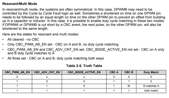
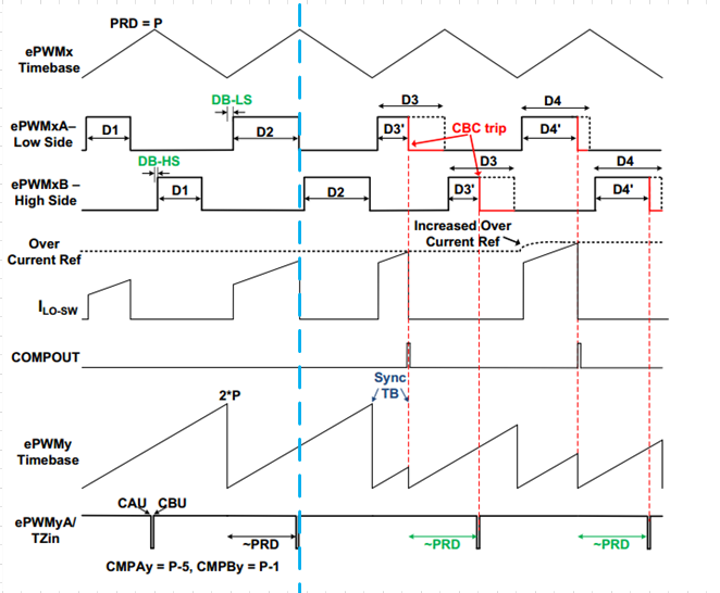
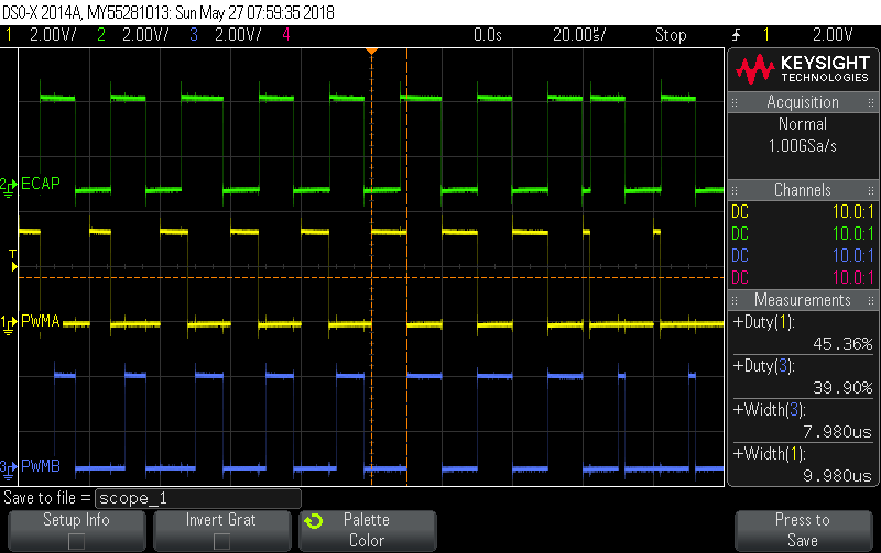
1. Duty matched feature while CBC occurs. I will configure the ePWMxA and ePWMxB with the same duty cycle, 180 degree phase. That means ePWMxB behind ePWMxA with half cycle. What I require is that when CBC occurs on ePWMxA, ePWMxB should keep the same pulse width with ePWMxA, and vice versa. How to configure the device to support this feature?

Below is the waveform what I want, CBC occurs on EPWM1A, EPWM1B should keep the same pulswidth with EPWM1A, is it possible?

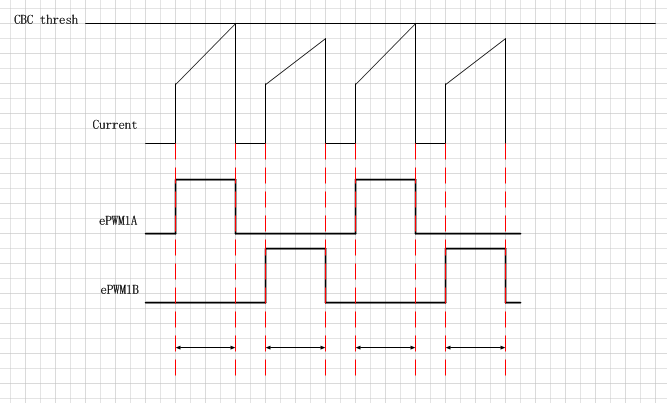
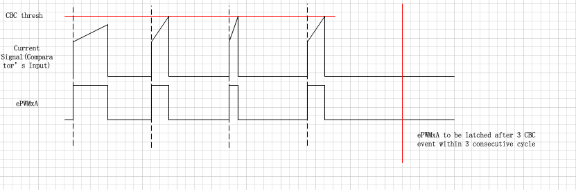
2. Require EPWM to be latched after receive a number of consecutive CBC events, and epwm should be tripped by CBC events.

Below waveform shows what I want, ePWMxA should be latched after 3 consecutive CBC event, is it possible?

3. What does mean of ‘Hardware-locked (synchronized) phase relationship on a cycle-by-cycle basis’ in f28004x’s TRM?

4. What does mean of ‘Programmable trip zone allocation of both cycle-by-cycle trip and one-shot trip on fault conditions.’ in f28004x’s TRM?

Thanks...

  • Hi Jack,

    1)

    This should be possible, but I'm not sure what the best way to achieve this would be. Maybe something along the lines of:
    *Over-current CBC trip event routed through the digital compare (DC) module
    *DC events cause an ePWM SOC event
    *DMA configured to trigger on ePWM SOC event. DMA copies the value of the ePWM time-base to compare register that causes ePWM1B to toggle low.

    2)

    See the end of the following thread for some advice about latching the ePWM after some number of CBC trips:
    e2e.ti.com/.../642772

    3)

    This just means that the hardware can force-load the TBPRD based on the TBPHS every cycle. This can be used to force two ePWM modules to maintain some fixed phase relationship.

    See the documentation for the timebase (TB) sub-module.

    4)

    The trip zones are events or faults that can cause a change in ePWM state.

    One-shot events occur and latch until cleared by the user. e.g. a critical over-current event clears all the ePWMs and they remain that way until the user re-starts the sytem.

    Cycle-by-cycle events are similar, but they can be automatically cleared by the start or end of the ePWM period (or both). e.g. an over-current event clears an ePWM phase until the ePWM time base reaches a period match

    You can route different events to either type of trip.
  • Hi Devin,

    For the #1, can you/ti provide a example code for me?

    For the #2, this is what I posted before with using firmware method, for 28004x device, that should have done a lots of enhancement, is there a hardware way to accomplish this?

    Thanks...
  • Hi Jack,

    1) We won't be able to write new code and provide it to you, but I'll check with the systems engineers to see if any of the existing power-supply kits have SW that uses this method or something similar.

    2) I don't think there is a HW way to accomplish this.  There are event prescalers, but these are not reset when the event does not occur.  Because of this, I think you need to count the consecutive events in the ISR and then SW trip if the limit is exceeded.  

  • Hey Devin,

    Thanks, please inform me if you have get the feedback from system engineers.

    If there is no reference code, it would be hard for me to get a exact and full feature as what I want. And I think this should be a common requirement for some DC/DC power supply, it will help other F28004x's user to get quick design.
  • Jack,

    1. We do not have anything to show exactly what you want.

    2. To point you to a more appropriate example that atleast has some aspect, I have a few questions for you

    i. On the first waveform xA duty is determined by CBC event only? Or is there a use case when CBC is not triggered and duty cycle is programmed to be be let;s say 30% and CBC is a special case..

    ii. If xA duty is determined by this fixed duty let's say 30% and CBC event occurs on 20% duty cycle, xB will be 20% or 30% ????

    I think if you can elaborate on normal behavior of PWM we can point you to a closer example for the waveform generation.
  • Also , in the waveform you showed xB never triggers a CBC event ??? is that true? or you do not want to count that even if it does?

    does that change xA duty then?
  • Hi Manish,

    i. On the first waveform xA duty is determined by CBC event only? Or is there a use case when CBC is not triggered and duty cycle is programmed to be be let;s say 30% and CBC is a special case..

    Jack-> No, without CBC triggered, the xA duty is determined by duty cycle programmed in COMx register. If the CBC triggered before the falling edge on A, then CBC determined the duty cycle, and xB should have the same pulse width with xA(where CBC triggered xA pull low).

    ii. If xA duty is determined by this fixed duty let's say 30% and CBC event occurs on 20% duty cycle, xB will be 20% or 30% ????

    Jack-> xB should be 20%.

    iii. Also , in the waveform you showed xB never triggers a CBC event ??? is that true? or you do not want to count that even if it does?

    Jack-> If the CBC triggers on xB, the xA should have the same duty cycle with xB. 

    Let me take example, if close loop output is 50% duty cycle, but CBC triggers xB on 30%, then xA should be 30%. 

  • Hi Manish,

    One of ti's device has this feature, here is the info for you. This TRM called it's duty match.

  • Jack,

    Thanks for your additional calrification on the use case.

    To assist you better can you be specific to which TRM and which device are you referring to for the above. I cannot find the same in F280049 TRM.

    Thanks
    Manish
  • Hi Manish,

    It's UCD3138, a digital power controller. Here is the TRM link:
    www.ti.com/.../sniu028
  • You can find this info at page 55 in this above manual.
  • Jack,

    We do not have the same PWM module as the UCD,

    I will have to discuss some options with our team internally and get back to you and to how to best implement what you are trying to run.

    regards
    Manish Bhardwaj
  • Thanks Manish.

    Looking forward to you/your team feedback. Thanks...
  • Jack,

    I think the duty matching should be possible. There is not a straightforward way to in the C2000 PWM to do it, but I think it can be accomplished through hardware.

    A few questions:

    a) Is there always going to be a deadtime between the A and B channels?
    b) How much difference can you tolerate between the two? Is a few cycles difference a big deal for your application?
    c) How are you counters setup? What are you compare values for the non-trip cases?

    Here's the first thought that comes to mind.

    You can setup an ECAP with a counter that is in sync with the PWM counter. This ECAP can detect the falling edge of your PWM signal by connecting the ECAP to the same pin as the A channel via the Input X-Bar. When the ECAP detects a falling edge, you can trigger a DMA transfer to transfer the ECAP counter value to the PWM COMPx register used for the falling edge of your B channel. If you can tolerate a few cycles of variation between the channels, I think this has a good chance of working.

    There are some "gotchas" to watch out for such as master aribtrations (CPU, DMA, CLA accesses). It also assumes the ECAP counter value is exactly the same value needed in your PWM cycle. I would actually consider using a separate EPWM module for each channel or using a simple APWM for the B channel.

    Regards,
    Kris
  • Hi Kris,

    This is a good proposal. Is there any reference code with this proposal?

    In my application case, under non-cbc trip case, the compare value comes from voltage loop result, the the compare register should be written by both CPU and CLA. Is there any risk?

    Here is my answer to your question:
    a) Is there always going to be a deadtime between the A and B channels?
    Jack: A and B has same pulse width with 180 phase degree. And there should be a dead-time between both channel.

    b) How much difference can you tolerate between the two? Is a few cycles difference a big deal for your application?
    Jack: What the tolerance of ECAP? I think +/-20ns should be OK.

    c) How are you counters setup? What are you compare values for the non-trip cases?
    Jack: The compare values comes from voltage loop final output under non-trip case.
  • Hi Jack,

    It is possible to implement CBC with duty matched behavior on the TMS320F28004x devices. I prepared the attached document a few years back. This document explains how you may achieve this when a CBC event occurs in the first half-cycle of the switching cycle and you want to use the same on-time in the following half-cycle. You will need an extra PWM resource to do this. If you want the same behavior if the CBC event occurs in the 2nd half cycle and want the same on-time in the following half-cycle, you may have to use another similar resource. 

    Let me know if you have any questions/concerns on this.

    Hrishi

    3678.Half-bridge_Charge-Sec_balance_E2E.pdf

  • Jack,

    I'm in the market for some F28004x hardware. Once I get my hands on some I can give it a try. It will likely be a couple of weeks before it arrives.

    I think I have a better solution than the original one though which someone at TI may be able to help with in the meantime.

    I want to setup a slave EPWM with the same period as your system PWM and always a 50% duty cycle. Rising edge on TBCTR=0. Then we can use the falling edge of the A channel to send a SYNC to the slave PWM to restart the TBCTR to 0. The falling edge of the slave PWM can trip the B channel on the system PWM. This setup isn't very straightforward and involves a number of internal connections through the EPWM and Input XBAR, but I have a high level of confidence it can work.

    Can you let us know which package you are using?

    As far as your counter setup, I am looking for up count, up down count, etc.

    Regards,
    Kris
  • Hi Hrishi,

    Really appreciate your help. It's a brilliant idea. Can you please share the reference code for me?

    As my high lighted by using blue dot line in below picture, if there is no CBC tips, is the EPWMxB is normal? Because of EPMWyA are connected to TZtrip, I think EPWMXB will be tripped at middle of period, how does this channel could be recovered immediately?

  • Another concern, this solution is for the fixed switch frequency power supply, if it's for LLC, the switch frequency is not fixed, is it still suitable?
  • Hi Kris,

    Really appreciate your help, it's really a brilliant idea. 100 pin will be used in my application.

    In this case, both master and slave EPWM should be used in up-mode, is it?
  • Hi Jack,

    I have hardware in the mail from TI. I'll write some sample code once I receive it.

    You won't actually be using a CBC. What you'll want to take a look at it is the new T1/T2 features in the action qualifier. It is a way to change the PWM output on a digital compare event without actually tripping the PWM. So in the case where your trip happens, the T1 event will force the A channel low before it reaches the compare event for the falling edge. That compare event will still take place, it just won't matter because the T1 event already made the PWM low. This also means that the B channel will not be tripped and the rising edge compare event still takes place. In the trip scenario, T2 will occur before the compare event for the falling edge of the B channel.

    Regards,

    Kris

  • Kris,

    Before you start going down this path, please keep in mind that the key requirement here is to use the on-time (result of a trip/T1/T2 event) in one half of the switching cycle in the 2nd half of the switching cycle. There is no CBC event in the 2nd half of the switching cycle. I don't think using T1/T2 is the solution. Please refer to my pdf file posted above.

    Jack,

    If there are no CBC events, EPWMxB will not be tripped and it will go to the programmed value. This is illustrated in the first two switching cycles in my drawing with programmed on-times equal to D1 and D2. This is possible because the PWM time-base y is synced on a trip event. Without a trip event time-base y will only be synced at the end of the PWMx period and will not shorten PWMxB on-time in that switching cycle.

    This solution works well for fixed frequency. It works for variable frequencies as well, but you have to be careful when and where the period and compare registers get updated. The ISR that updates these values must be synchronized with the switching cycle.

    I do not have code that can be shared at this time. The configuration explained in my previous post is all that you would need to realize this functionality. Please let me know if you need help once you start configuring the PWMs this way.

    Hrishi

  • Hrishi,

    I missed the PDF in your previous reply. That looks like a good solution very similar to what I was thinking. How are you getting the EPWMx back to the PWM being used in the system to cause the trip in the second half of the cycle? Are you taking it to a pin and routing it back through the X-Bars?

    In my solution, I was going to be creating the T2 event in the second half of the cycle with a PWM which looks similar to what you proposed. I think it could also be a CBC. One or both (T1/T2 or CBC) of them will work would just need to get further into the details to try it.

    Regards,

    Kris

  • Yes, taking it to a pin. CBC or T1/T2 doesn't matter much.

    Hrishi
  • I was able to do this without using an extra pin. I used the method described previously (T1/T2 events creating falling edges, 50% duty cycle on PWM), but instead of using an EPWM I used an ECAP. The benefit of the ECAP is you can route it internally to the EPWM via the EPWM X-BAR.

    I brought the ECAP to a GPIO as well for demonstration purposes, but it can be removed from the GPIO and this will still work.  I included a waveform below. What you'll see is that as the A channel duty cycle changes the B channel automatically matches it in the same PWM cycle. In the example code, I'm just modifying CMPA to change the pulse-width of PWMA, but since the ECAP is syncing off of the falling edge of PWM1A this will work no matter what causes the falling edge (CMPA, CBC, T1).

    This code was actually created on the F28379D launchpad, but the solution is still applicable to F28004x. You can copy this code into an example project and just have a few minor things to change to get up and running.

    Are there any known silicon issues with syncing the ECAP in APWM mode? If the CTRPHS was > 0 (in this case I used 8) either some of the sync events were missed or the rising edge event missed. You can see in the red box below that the ECAP is missing a pulse despite the falling edge of PWMA. It will not affect the solution posted above as it works fine with CTRPHS = 0. However, it looks like it needs further investigation on why this is happening. You can replicate this by taking the example code attached and changing ECap1Regs.CTRPHS = 8.

    Example code is attached. Enjoy!

    /* Example software demonstrating duty cycle matching with the EPWM and ECAP modules
     * This example requires 1 ECAP in APWM per EPWM module which requires the duty matching feature
     *
     * In this example, the EPWM ISR modifies CMPA to demonstrate the behavior of the
     * B channel pulse width as the A channel pulse width is changed. This is simulating a
     * CBC event for the purposes of this example.
     *
     * The ECAP is set to a 50% duty cycle with the same period as the PWM.
     * Whenever PWMA has a falling edge, the ECAP receives a SYNC and begins counting
     * at CTR=0. The falling edge of the ECAP causes a T2 event in the EPWM to create
     * a falling edge on EPWMB. This effectively creates a duty matching feature in the EPWM.
     *
     * In this example, ECAP1OUT is shown on GPIO5 for demonstration purposes only! An extra
     * pin is not required as it is routed directly to the EPWM through the EPWM X-BAR.
     *
     * Kris Parrent
     * May 26th, 2018
     * kris@realcoders.com
     */
    //
    // Included Files
    //
    #include "F28x_Project.h"
    
    //
    //  Function Prototypes
    //
    void InitECapAPWM(void);
    void InitEPwm1Example(void);
    interrupt void epwm1_isr(void);
    
    //
    // Main
    //
    void main(void)
    {
    //
    // Step 1. Initialize System Control:
    // PLL, WatchDog, enable Peripheral Clocks
    // This example function is found in the F2837xD_SysCtrl.c file.
    //
        InitSysCtrl();
    
        EALLOW;
        ClkCfgRegs.PERCLKDIVSEL.bit.EPWMCLKDIV = 0; // Set EPWMCLK = SYSCLK for this example. Your device should run at 100 MHz or less.
        EDIS;
    //
    // Step 2. Initialize GPIO:
    // This example function is found in the F2837xD_Gpio.c file and
    // illustrates how to set the GPIO to it's default state.
    //
    //    InitGpio();
    
    //
    // Enable PWM1, PWM2 and PWM3
    //
        EALLOW;
        CpuSysRegs.PCLKCR2.bit.EPWM1=1;
        CpuSysRegs.PCLKCR3.bit.ECAP1 = 1;
        EDIS;
    
    //
    // For this case just init GPIO pins for ePWM1, ePWM2, ePWM3
    // These functions are in the F2837xD_EPwm.c file
    //
        InitEPwm1Gpio();
        InitAPwm1Gpio();
    
        EALLOW;
        SyncSocRegs.SYNCSELECT.bit.ECAP1SYNCIN = 6; // ECAP1SYNCIN = EXTSYNCIN2 = INPUTXBAR6
        InputXbarRegs.INPUT6SELECT = 0;             // GPIO0 = EPWM1A
        GpioCtrlRegs.GPAINV.bit.GPIO0 = 1;          // Invert Input on GPIO0 (Sync chain is active high, want sync on falling edge)
    
        // Set ECAP1.OUT to TRIP4 on EPWM X-Bar
        EPwmXbarRegs.TRIP4MUX0TO15CFG.bit.MUX0 = 3; // ECAP1OUT
        EPwmXbarRegs.TRIP4MUXENABLE.bit.MUX0 = 1;   // Enable MUX0
        EDIS;
    //
    // Step 3. Clear all interrupts and initialize PIE vector table:
    // Disable CPU interrupts
    //
        DINT;
    
    //
    // Initialize the PIE control registers to their default state.
    // The default state is all PIE interrupts disabled and flags
    // are cleared.
    // This function is found in the F2837xD_PieCtrl.c file.
    //
        InitPieCtrl();
    
    //
    // Disable CPU interrupts and clear all CPU interrupt flags:
    //
        IER = 0x0000;
        IFR = 0x0000;
    
    //
    // Initialize the PIE vector table with pointers to the shell Interrupt
    // Service Routines (ISR).
    // This will populate the entire table, even if the interrupt
    // is not used in this example.  This is useful for debug purposes.
    // The shell ISR routines are found in F2837xD_DefaultIsr.c.
    // This function is found in F2837xD_PieVect.c.
    //
        InitPieVectTable();
    
        EALLOW;
        PieVectTable.EPWM1_INT = &epwm1_isr;
        EDIS;
    //
    // For this example, only initialize the ePWM
    //
        EALLOW;
        CpuSysRegs.PCLKCR0.bit.TBCLKSYNC = 0;
        EDIS;
    
        InitEPwm1Example();
        InitECapAPWM();
    
        EALLOW;
        CpuSysRegs.PCLKCR0.bit.TBCLKSYNC = 1;
        EDIS;
    
    //
    // Step 4. User specific code, enable interrupts:
    //
    // Enable CPU INT3 which is connected to EPWM1-3 INT:
    //
        IER |= M_INT3;
    
    //
    // Enable EPWM INTn in the PIE: Group 3 interrupt 1-3
    //
        PieCtrlRegs.PIEIER3.bit.INTx1 = 1;
    
    //
    // Enable global Interrupts and higher priority real-time debug events:
    //
        EINT;  // Enable Global interrupt INTM
        ERTM;  // Enable Global realtime interrupt DBGM
    
    
    //
    // Step 5. IDLE loop. Just sit and loop forever (optional):
    //
        for(;;)
        {
            asm ("  NOP");
        }
    }
    
    interrupt void epwm1_isr()
    {
        if(EPwm1Regs.CMPA.bit.CMPA != 499)
        {
            EPwm1Regs.CMPA.bit.CMPA += 100;
        }else
        {
            EPwm1Regs.CMPA.bit.CMPA = 99;
        }
    
        //
        // Clear INT flag for this timer
        //
        EPwm1Regs.ETCLR.bit.INT = 1;
    
        //
        // Acknowledge this interrupt to receive more interrupts from group 3
        //
        PieCtrlRegs.PIEACK.all = PIEACK_GROUP3;
    }
    //
    // InitEPwm1Example - Initialize EPWM1 values
    //
    void InitEPwm1Example()
    {
        EALLOW;
       //
       // Setup TBCLK
       //
       EPwm1Regs.TBCTL.bit.CTRMODE = TB_COUNT_UP; // Count up
       EPwm1Regs.TBPRD = 999;                     // Set timer period
       EPwm1Regs.TBCTL.bit.PHSEN = TB_DISABLE;    // Disable phase loading
       EPwm1Regs.TBPHS.bit.TBPHS = 0x0000;        // Phase is 0
       EPwm1Regs.TBCTR = 0x0000;                  // Clear counter
       EPwm1Regs.TBCTL.bit.SYNCOSEL = 2;          // Generate SYNCO on CMPB (falling edge of A channel)
    
       // Set PWM dividers to /1
       EPwm1Regs.TBCTL.bit.HSPCLKDIV = 0;
       EPwm1Regs.TBCTL.bit.CLKDIV = 0;
    
       EPwm1Regs.ETSEL.bit.INTSEL = ET_CTR_ZERO;     // Select INT on Zero event
       EPwm1Regs.ETSEL.bit.INTEN = 1;                // Enable INT
       EPwm1Regs.ETPS.bit.INTPRD = ET_3RD;           // Generate INT on 3rd event
    
       //
       // Setup shadow register load on ZERO
       //
       EPwm1Regs.CMPCTL.bit.SHDWAMODE = CC_SHADOW;
       EPwm1Regs.CMPCTL.bit.SHDWBMODE = CC_SHADOW;
       EPwm1Regs.CMPCTL.bit.LOADAMODE = CC_CTR_ZERO;
       EPwm1Regs.CMPCTL.bit.LOADBMODE = CC_CTR_ZERO;
    
       //
       // Set Compare values
       //
       EPwm1Regs.CMPA.bit.CMPA = 499;     // Set compare A value
       EPwm1Regs.CMPB.bit.CMPB = 499;     // Set compare A value
    
       //
       // Set actions
       //
       EPwm1Regs.AQCTLA.bit.ZRO = AQ_SET;        // Set PWM1A on Zero
       EPwm1Regs.AQCTLA.bit.CAU = AQ_CLEAR;      // Clear PWM1A on event A,
                                                 // up count
    
       EPwm1Regs.AQCTLB.bit.PRD = AQ_CLEAR;      // Set PWM1B on Zero
       EPwm1Regs.AQCTLB.bit.CBU = AQ_SET;        // Clear PWM1B on event B,
    
       EPwm1Regs.AQTSRCSEL.bit.T2SEL = 3;        // DCBEVT2
       EPwm1Regs.AQCTLB2.bit.T2U = 1;            // Clear B channel on T2 event
    
       // Configure Digital Compare for ECAP1.OUT on TRIP4
       EPwm1Regs.DCTRIPSEL.bit.DCBLCOMPSEL = 3; // DCBL = TRIP4
       EPwm1Regs.DCBCTL.bit.EVT1SRCSEL = 0;
       EPwm1Regs.TZDCSEL.bit.DCBEVT2 = 3;       // DCBEVT1 = DCBL low DCBH don't care
       EPwm1Regs.TZCTL.bit.DCBEVT2 = 3;         // Do nothing to EPWMB on DCBEVT2
    
       EDIS;
    }
    
    void InitECapAPWM()
    {
        //
        // Setup APWM mode on CAP1, set period and compare registers
        //
           ECap1Regs.ECCTL2.bit.CAP_APWM = 1;       // Enable APWM mode
           ECap1Regs.ECCTL2.bit.APWMPOL = 0;        // Active high polarity
           ECap1Regs.ECCTL2.bit.SYNCI_EN = 1;       // Enable SYNCI
           ECap1Regs.CTRPHS = 0;
           ECap1Regs.CAP1 = 999;                    // Set Period value
           ECap1Regs.CAP2 = 487;                    // Set Compare value
                                                    // This should be approximately 50% duty cycle
                                                    // It is slightly shorter to account for propagation
                                                    // and latch delays from the ECAP through EPWM
           ECap1Regs.ECCTL2.bit.TSCTRSTOP = 1;      // Start counter
    
    }
    
    //
    // End of file
    //
    

    Regards,

    Kris

  • Really appreciate your help on this.
  • Thanks for your effort.