This thread has been locked.

If you have a related question, please click the "Ask a related question" button in the top right corner. The newly created question will be automatically linked to this question.

TMS320F280049: Electrical characteristics difference on F280049’s analog pins

Part Number: TMS320F280049

Hi expert,

My customer uses F28004x in multiple of their projects. They have found differences on electrical characteristics of different analog pins.

This problem only occurs when source impedence for ADC input is high (several kilo ohms) for they didn’t use any amplifier before ADC input. ( this is not key point) The problem they found is: in situation above, analog signal on several ADCs channels will draw external signal (prevent them from rising to theoretical value). The problem occurs on blow pins (100pin package): Pin36 and Pin44. Not occurs on below pins: Pin28 and Pin35.

Could you tell the differences internally?

Thanks

Sheldon

  • Hi Sheldon,

    Using an input with high input impedance but no buffer can cause a variety of somewhat unpredictable errors.

    Given the customer's S+H duration, external impedance, the ADC input characteristics in the datasheet table "Input Model Parameters", and the equations in the TRM section of the ADC chapter "Choosing an Acquisition Window Duration" you should be able to solve for the settling error.

    I don't think we have an issue unless the observed variance in accuracy between the channels is larger than the predicted settling error.
  • Hi Devin,

    Even on my side I am not able to reproduce their issue with high impedence source for the time being. (I am still working with them and trying to reproduce this on control card)
    But, could you confirm that if I only use ADC function (with PGA disabled) the electrical characteristic seeing from outside of different ADC pins are identical? ( e.g. for 100 pin package, pin36, pin28, pin44 and pin35 are identical from outside )

    Thanks
    Sheldon
  • Hi Sheldon,

    There will be some minor variation between the channels. This variation should not affect the results as long as the driving circuit + S&H has been designed to meet the worst case specified in the ADC input model (which should take into account worst-case channel characterisitcs). If the driving circuit is not well designed for the ADC input characteristics then you could see minor channel variations, channel sequencing, device-to-device variation, etc. show up as noticeable error when they should be normally insignificant.
  • Hi Devin,

    I get more useful information from customer, this issue seems related to F280049's working status or whole system layout. I will update more details once I get them.

    Briefly, on two of their running projects with F280049, some ADC pins will significantly draw voltage from like 2.5V to 2.2V in "some working states". BTW, this issue never happens on some other ADC pins of the same device. Tricky.

    Thanks

    Sheldon

  • Hi Devin,


    This problem happens when F280049’s ADC sampling DC voltage output. Customer engineer use resistors to divide (1) the high voltage DC down and sample it with F280049’s ADC. They find that in some special working point (2), some ADC pins will draw the external voltage to some low level some others will not (3). I have paying much effort helping them with this problem, we tried many things, some helps, some are not (4). I also tried to reproduce it on F280049 control card with quite small sample window and large source impedance, but in vain. 


    (1) See circuitry below

    (2) Output current = 7~9 A, Battery voltage > 460 V, Switching frequency = 250 kHz

    (3) Normal (Theoretical) external voltage is 2.5V, draw to 2.2V when connecting to ADC pin, back to normal value when cutting this trace. Voltage is consistently drawing down even the ADC is not working.

    (4)

    Failed attempts

    Switching R2371 to 470Ω

    Changing capacitor C2443

    Changing voltage sample hold time (from original 10 to much bigger value)

    Useful attempts:

    Add voltage follower before ADC

    Changing ADC from A4 (pin 36) to C5 (pin 28) (This is the key reason for I consider it as an EMI related issue)


    Thanks

    Sheldon

  • Hi Sheldon,

    The effective source resistance on the A4 channel is (3.65kohm || 650kohm) + 1kohm = 4.63kohm.  This would definitely be considered very very high.  

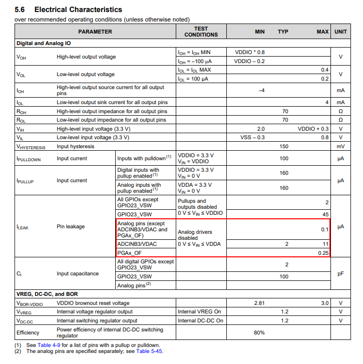
    If the input drops 0.3V, then the parasitic current is 0.3V/4.63kohm =  65uA.   This is much larger than the specified leakage current (see below) so either there is another path for static current dissipation or the input has been damaged via ESD or EOS.  

    Note that during active operation we might expect and additional current of up to 250kHz*(12.5pF*2.5V) = 7.8uA.  This might result in an additional 35mV or so drop.  

    Do you see this on the ControlCard or Launchpad with an equivalent source impedance, or only the customer's system?  Is this only in one system, or many?  This seems like ESD or EOS damage to me.  I see that there is an input protection diode on the input side, but there is no series resistance after the diode.  Series resistance between the diodes is needed to steer current away from the internal protection diodes to the external diodes in case of an over-voltage event.  Alternately, is it possible the input went below VSSA at any point?  

    I'm also not understanding how the current sense works here.  Is there a current sense resistor somewhere to convert the 7-9A to a voltage?  

  • Hi Devin,

    Thanks for your detailed explanation. I will provides you with more details I have. Before that, could you help me with how does "250kHz*(12.5pF*2.5V) = 7.8uA" comes from?

    Q: Do you see this on the ControlCard or Launchpad with an equivalent source impedance, or only the customer's system? 

    A: No, I tested on F280049 control card with same package, same pins. Even with a extreme source impedance will not reproduce. Though my sampling rate is not as high as they are. I think this is not important for they states that this problem occurs even when ADC is not sampling. So, only on customer's system.

    Q: Is this only in one system, or many? 

    A: Many. Same phenomenon on two different projects and more than one boards for each project.

    Q: is it possible the input went below VSSA at any point?  

    A: I need to check with them. For this is output of DCDC (secondary side), there is not much chance go below VSSA.

    Q: Is there a current sense resistor somewhere to convert the 7-9A to a voltage? 

    A: Actually I didn't mention it clearly. 7 to 9 A indicates output power of this machine (some working state of this machine), this ADC pins is sampling the output voltage using resistor divider, not for current sensing.

    For you consider there could be some damage to ESD. They didn't do tests such a surge on these machines.

    Could it be some EMI problem?

    Thanks

    Sheldon

  • Hi Sheldon,

    Quick comments:
    The S+H capacitor is 12.5pF. In the worst case the external source will have to charge it 0 to 2.5V on each sample. Samples are occurring at 250kHz.

    Mathematically C = Q/V and I = Q/t
    C = 12.5pF
    V = 2.5V
    So Q = 12.5pF*2.5V
    t = 1/250kHz
    So I = 12.5pF*2.5V*250kHz

    I don't see how this could be an EMI problem, unless you are suggesting that EMI somehow induced a transient ESD or EOS event?
  • Hi Devin,
    We will internally do more communication with them to find more facts on this issue.
    Thanks
    Sheldon