Other Parts Discussed in Thread: C2000WARE
I am using PCAN to transmit message which is set at 1M bits/sec and I am using ECAN on F28069 as Receiver end
ECanaShadow.CANBTC.bit.BRPREG = 1;
ECanaShadow.CANBTC.bit.TSEG2REG = 2;
ECanaShadow.CANBTC.bit.TSEG1REG = 10; , these are the values I have set on ecan SIDE TO SET IT TO 1M BITS/SEC.I am sending data from PCAN at 1ms cycle time.
#include "DSP28x_Project.h" // Device Headerfile and Examples Include File
#include "F2806x_Ecan.h"
long RXCOUNT = 0;
long i;
volatile struct ECAN_REGS ECanaRegs;
volatile struct ECAN_MBOXES ECanaMboxes;
void MBXwrA(void); // This function initializes all 32 MBOXes of CAN-A
void mailbox_read(void);
Uint32 TestMbox1 = 0;
Uint32 TestMbox2 = 0;
Uint32 TestMbox3 = 0;
main()
{
/* Create a shadow register structure for the CAN control registers. This is
needed, since, only 32-bit access is allowed to these registers. 16-bit access
to these registers could potentially corrupt the register contents. This is
especially true while writing to a bit (or group of bits) among bits 16 - 31 */
struct ECAN_REGS ECanaShadow;
struct ECAN_MBOXES ECanaMboxes;
// Step 1. Initialize System Control:
// PLL, WatchDog, enable Peripheral Clocks
// This example function is found in the DSP280x_SysCtrl.c file.
InitSysCtrl();
/* Initialize the CAN module */
// ECanaMboxes.MBOX25.MSGID.all = 0x001;
//ECanaMboxes.MBOX25.MSGCTRL.bit.DLC = 8;
//ECanaMboxes.MBOX25.MDL.all = 0;
//ECanaMboxes.MBOX25.MDH.all = 0;
MBXwrA();
InitECan();
InitECanGpio();
EALLOW;
/* Zero out (or initialize) the entire MBX RAM area */
// MBXwrB();
/* Write to the MSGID field 0f CAN-A - MBX number is written as its MSGID */
ECanaMboxes.MBOX1.MSGID.all = 0x11000000;
/* Configure CAN-A Mailboxes as Receive mailboxes */
ECanaShadow.CANMD.all = ECanaRegs.CANMD.all;
ECanaShadow.CANMD.bit.MD1 = 1;
//ECanaShadow.CANMD.all = 0xFFFFFFFF;
ECanaRegs.CANMD.all = ECanaShadow.CANMD.all;
/* Enable Mailboxes */
ECanaShadow.CANME.all = ECanaRegs.CANME.all;
//ECanaShadow.CANME.all = 0xFFFFFFFF;
ECanaShadow.CANME.bit.ME1 = 1;
ECanaRegs.CANME.all = ECanaShadow.CANME.all;
/* Begin receiving */
while(1)
{
int j;
while(ECanaRegs.CANRMP.all != 0xFFFFFFFF) {} // Wait for all RMPn to be set..
ECanaRegs.CANRMP.all = 0xFFFFFFFF; // Clear all RMPn bits and start
RXCOUNT++ ; // all over again...
//Read from Receive mailboxes and begin checking for data */
// for(j=0; j<32; j++) // Read & check 16 mailboxes
mailbox_read(); // This func reads the indicated mailbox data
if(RXCOUNT==1000){break;}
}
ESTOP0;
}
/* Zero-out the MBX RAM of CAN-A */
void MBXwrA()
{
int j;
volatile struct MBOX *Mailbox = (void *) 0x6100;
for(j=0; j<32; j++)
{
// Mailbox->MSGID.all = 0;
Mailbox->MSGCTRL.all = 0;
Mailbox->MDH.all = 0;
Mailbox->MDL.all = 0;
Mailbox = Mailbox + 1;
}
}
void mailbox_read(void)
{
volatile struct MBOX *Mailbox;
Mailbox = &ECanaMboxes.MBOX1 ;
TestMbox1 = Mailbox->MDL.byte.BYTE1; // = 0x9555AAAn (n is the MBX number)
TestMbox2 = Mailbox->MDH.byte.BYTE4; // = 0x89ABCDEF (a constant)
//TestMbox3 = Mailbox->MSGID.all;// = 0x9555AAAn (n is the MBX number)
} // MSGID of a rcv MBX is transmitted as the MDL data.
For CAN Intialization below is the code:
//###########################################################################
//
// FILE: F2806x_ECan.ayushi
//
// TITLE: F2806x Enhanced CAN Initialization & Support Functions.
//
//###########################################################################
// $TI Release: F2806x C/C++ Header Files and Peripheral Examples V1.20 $
// $Release Date: November 30, 2011 $
//###########################################################################
#include "F2806x_Device.h" // F2806x Headerfile Include File
#include "F2806x_Examples.h" // F2806x Examples Include File
#include "F2806x_ECan.h"
#include "F2806x_Gpio.h"
//---------------------------------------------------------------------------
// InitECan:
//---------------------------------------------------------------------------
// This function initializes the eCAN module to a known state.
//
#if DSP28_ECANA
void InitECan(void)
{
InitECana();
}
#endif
#if DSP28_ECANA
void InitECana(void) // Initialize eCAN-A module
{
/* Create a shadow register structure for the CAN control registers. This is
needed, since only 32-bit access is allowed to these registers. 16-bit access
to these registers could potentially corrupt the register contents or return
false data. */
volatile struct ECAN_REGS ECanaShadow;
volatile struct ECAN_REGS ECanaRegs;
volatile struct ECAN_MBOXES ECanaMboxes;
EALLOW; // EALLOW enables access to protected bits
/* Configure eCAN RX and TX pins for CAN operation using eCAN regs*/
ECanaShadow.CANTIOC.all = ECanaRegs.CANTIOC.all;
ECanaShadow.CANTIOC.bit.TXFUNC = 1;
ECanaRegs.CANTIOC.all = ECanaShadow.CANTIOC.all;
ECanaShadow.CANRIOC.all = ECanaRegs.CANRIOC.all;
ECanaShadow.CANRIOC.bit.RXFUNC = 1;
ECanaRegs.CANRIOC.all = ECanaShadow.CANRIOC.all;
/* Configure eCAN for HECC mode - (reqd to access mailboxes 16 thru 31) */
// HECC mode also enables time-stamping feature
ECanaShadow.CANMC.all = ECanaRegs.CANMC.all;
ECanaShadow.CANMC.bit.SCB = 1;
ECanaRegs.CANMC.all = ECanaShadow.CANMC.all;
/* Initialize all bits of 'Message Control Register' to zero */
// Some bits of MSGCTRL register come up in an unknown state. For proper operation,
// all bits (including reserved bits) of MSGCTRL must be initialized to zero
ECanaMboxes.MBOX0.MSGCTRL.all = 0x00000000;
ECanaMboxes.MBOX1.MSGCTRL.all = 0x00000000;
ECanaMboxes.MBOX2.MSGCTRL.all = 0x00000000;
ECanaMboxes.MBOX3.MSGCTRL.all = 0x00000000;
ECanaMboxes.MBOX4.MSGCTRL.all = 0x00000000;
ECanaMboxes.MBOX5.MSGCTRL.all = 0x00000000;
ECanaMboxes.MBOX6.MSGCTRL.all = 0x00000000;
ECanaMboxes.MBOX7.MSGCTRL.all = 0x00000000;
ECanaMboxes.MBOX8.MSGCTRL.all = 0x00000000;
ECanaMboxes.MBOX9.MSGCTRL.all = 0x00000000;
ECanaMboxes.MBOX10.MSGCTRL.all = 0x00000000;
ECanaMboxes.MBOX11.MSGCTRL.all = 0x00000000;
ECanaMboxes.MBOX12.MSGCTRL.all = 0x00000000;
ECanaMboxes.MBOX13.MSGCTRL.all = 0x00000000;
ECanaMboxes.MBOX14.MSGCTRL.all = 0x00000000;
ECanaMboxes.MBOX15.MSGCTRL.all = 0x00000000;
ECanaMboxes.MBOX16.MSGCTRL.all = 0x00000000;
ECanaMboxes.MBOX17.MSGCTRL.all = 0x00000000;
ECanaMboxes.MBOX18.MSGCTRL.all = 0x00000000;
ECanaMboxes.MBOX19.MSGCTRL.all = 0x00000000;
ECanaMboxes.MBOX20.MSGCTRL.all = 0x00000000;
ECanaMboxes.MBOX21.MSGCTRL.all = 0x00000000;
ECanaMboxes.MBOX22.MSGCTRL.all = 0x00000000;
ECanaMboxes.MBOX23.MSGCTRL.all = 0x00000000;
ECanaMboxes.MBOX24.MSGCTRL.all = 0x00000000;
ECanaMboxes.MBOX25.MSGCTRL.all = 0x00000000;
ECanaMboxes.MBOX26.MSGCTRL.all = 0x00000000;
ECanaMboxes.MBOX27.MSGCTRL.all = 0x00000000;
ECanaMboxes.MBOX28.MSGCTRL.all = 0x00000000;
ECanaMboxes.MBOX29.MSGCTRL.all = 0x00000000;
ECanaMboxes.MBOX30.MSGCTRL.all = 0x00000000;
ECanaMboxes.MBOX31.MSGCTRL.all = 0x00000000;
// TAn, RMPn, GIFn bits are all zero upon reset and are cleared again
// as a matter of precaution.
ECanaRegs.CANTA.all = 0xFFFFFFFF; /* Clear all TAn bits */
ECanaRegs.CANRMP.all = 0xFFFFFFFF; /* Clear all RMPn bits */
ECanaRegs.CANGIF0.all = 0xFFFFFFFF; /* Clear all interrupt flag bits */
ECanaRegs.CANGIF1.all = 0xFFFFFFFF;
/* Configure bit timing parameters for eCANA*/
ECanaShadow.CANMC.all = ECanaRegs.CANMC.all;
ECanaShadow.CANMC.bit.CCR = 1 ; // Set CCR = 1
ECanaRegs.CANMC.all = ECanaShadow.CANMC.all;
// Wait until the CPU has been granted permission to change the configuration registers
do
{
ECanaShadow.CANES.all = ECanaRegs.CANES.all;
} while(ECanaShadow.CANES.bit.CCE != 1 ); // Wait for CCE bit to be set..
ECanaShadow.CANBTC.all = 0;
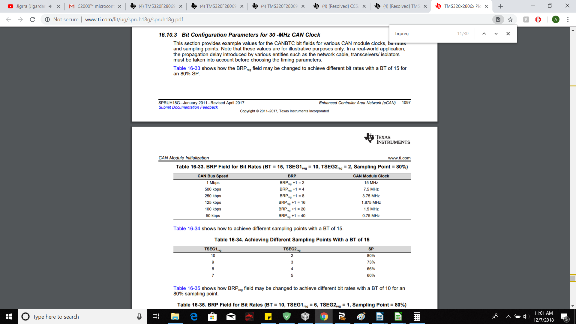
/* The following block is for 80 MHz SYSCLKOUT. (40 MHz CAN module clock Bit rate = 1 Mbps
See Note at end of file. */
ECanaShadow.CANBTC.bit.BRPREG = 1;
ECanaShadow.CANBTC.bit.TSEG2REG = 2;//4
ECanaShadow.CANBTC.bit.TSEG1REG = 10;//13
ECanaShadow.CANBTC.bit.SAM = 1;
ECanaRegs.CANBTC.all = ECanaShadow.CANBTC.all;
ECanaShadow.CANMC.all = ECanaRegs.CANMC.all;
ECanaShadow.CANMC.bit.CCR = 0 ; // Set CCR = 0
ECanaRegs.CANMC.all = ECanaShadow.CANMC.all;
//ECanaShadow.CANES.bit.CCE = 1;
// Wait until the CPU no longer has permission to change the configuration registers
do
{
ECanaShadow.CANES.all = ECanaRegs.CANES.all;
} while(ECanaShadow.CANES.bit.CCE != 0); // Wait for CCE bit to be cleared..
/* Disable all Mailboxes */
ECanaRegs.CANME.all = 0; // Required before writing the MSGIDs
EDIS;
}
#endif // endif DSP28_ECANA
//---------------------------------------------------------------------------
// Example: InitECanGpio:
//---------------------------------------------------------------------------
// This function initializes GPIO pins to function as eCAN pins
//
// Each GPIO pin can be configured as a GPIO pin or up to 3 different
// peripheral functional pins. By default all pins come up as GPIO
// inputs after reset.
//
// Caution:
// Only one GPIO pin should be enabled for CANTXA operation.
// Only one GPIO pin shoudl be enabled for CANRXA operation.
// Comment out other unwanted lines.
#if DSP28_ECANA
void InitECanGpio(void)
{
InitECanaGpio();
}
#endif
#if DSP28_ECANA
void InitECanaGpio(void)
{
EALLOW;
/* Enable internal pull-up for the selected CAN pins */
// Pull-ups can be enabled or disabled by the user.
// This will enable the pullups for the specified pins.
// Comment out other unwanted lines.
GpioCtrlRegs.GPAPUD.bit.GPIO30 = 0; // Enable pull-up for GPIO30 (CANRXA)
GpioCtrlRegs.GPAPUD.bit.GPIO31 = 0; // Enable pull-up for GPIO31 (CANTXA)
/* Set qualification for selected CAN pins to asynch only */
// Inputs are synchronized to SYSCLKOUT by default.
// This will select asynch (no qualification) for the selected pins.
GpioCtrlRegs.GPAQSEL2.bit.GPIO30 = 3; // Asynch qual for GPIO30 (CANRXA)
/* Configure eCAN-A pins using GPIO regs*/
// This specifies which of the possible GPIO pins will be eCAN functional pins.
GpioCtrlRegs.GPAMUX2.bit.GPIO30 = 1; // Configure GPIO30 for CANRXA operation
GpioCtrlRegs.GPAMUX2.bit.GPIO31 = 1; // Configure GPIO31 for CANTXA operation
EDIS;
}
#endif // endif DSP28_ECANA
/* Note: Bit timing parameters must be chosen based on the network parameters such as
the sampling point desired and the propagation delay of the network. The propagation
delay is a function of length of the cable, delay introduced by the
transceivers and opto/galvanic-isolators (if any).
The parameters used in this file must be changed taking into account the above mentioned
factors in order to arrive at the bit-timing parameters suitable for a network.
*/
//===========================================================================
// End of file.
//===========================================================================