This thread has been locked.

If you have a related question, please click the "Ask a related question" button in the top right corner. The newly created question will be automatically linked to this question.

TMS320F28377D: DCSM problem

Part Number: TMS320F28377D

I tried to secure my project using DCSM according to the example project "blinky_with_DCSM" provided by TI. But it failed when I loaded the program using CCS(Version 7.3.0.00019). The console window outputs the message "

C28xx_CPU1: Error during Flash programming (Flash algorithm returned error code). Operation cancelled.
C28xx_CPU1: File Loader: Memory write failed: Unknown error
C28xx_CPU1: GEL: File: G:\ProductProject\Project\CPU1\OutputFiles\XXXX_V1_US_CPU1_FW3_NE.out: Load failed.

"

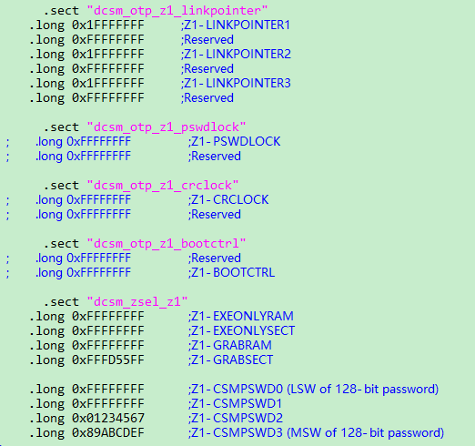
The "DCSM_Z1_ZoneSelectBlock.asm" code is posted below,

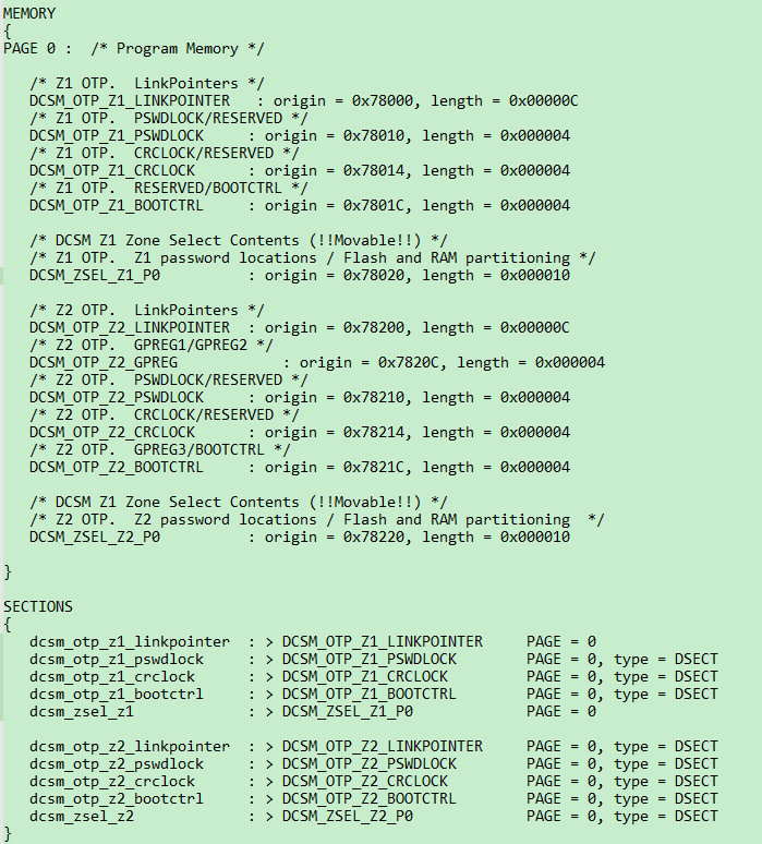
The "2837xD_dcsm_lnk_cpu1.cmd" is posted below,

  • Update:
    1. The Z1-LINKPOINT1~3 can be programmed successfully. I verified that with 0xFFFFFFFE.
    2. The Z1-GRABSECT and Z1-CSWPSWD can't be programmed with always the value 0xFFFFFFFF.
  • Hi,

    I guess you've programmed Z1-GRABSECT and Z1-CSWPSWD with FF's already? If so, then since these are one time programmable you need to advance to DCSM_ZSEL_Zx_P1, P2 or higher.

    Edward
  • Hi Vesgine,

    As mentioned by Edward, if you have programmed any value earlier (even with value 0xFFFF_FFFF) then corresponding ECC values will get programmed hence any new value with (which will have new ECC value) will not get programmed (ECC is also OTP). In this case you need to advance the link pointer to select next Zone Select Block and program the new values there.

    Regards,
    Vivek Singh
  • As you suggested, I changed my code above. However, It still failed with the same console output

    C28xx_CPU1: Error during Flash programming (Flash algorithm returned error code). Operation cancelled.
    C28xx_CPU1: File Loader: Memory write failed: Unknown error
    C28xx_CPU1: GEL: File: G:\ProductProject\Project\CPU1\OutputFiles\XXXX_V1_NE_CPU1_FW3.out: Load failed.

    The DCSM Z1 register value are shown below.

    The ECC value for DCSM OTP are shown below.

  • I found that the Flash ECC locations for DCSM OTP were programmed already. Since these ECC memories are also OTP, So I can't reprogram DCSM  OTP. Is that right?

    So if I want to secure the DSP with DCSM, I should program the DCSM OTP only for the first time. After that, if I want to update the program without changing the password, the new project should remove the file "DCSM_Z1_ZoneSelectBlock.asm" or comment .long words. Is that right?

    I program another new chip with the same program as my last post successfully. 

    The ECC memory value are shown below.

    I programmed  0x78040~0x7804F, the result is 0x1071009 and 0x107100A are programmed. So what's the mapping between the DCSM OTP memory and ECC OTP memory? 

  • Hi.

    I found that the Flash ECC locations for DCSM OTP were programmed already. Since these ECC memories are also OTP, So I can't reprogram DCSM  OTP. Is that right?

    That is correct.

    So if I want to secure the DSP with DCSM, I should program the DCSM OTP only for the first time. After that, if I want to update the program without changing the password, the new project should remove the file "DCSM_Z1_ZoneSelectBlock.asm" or comment .long words. Is that right?

    Yes, it is better to remove it though if values are same then you should not see any error.

    I programmed  0x78040~0x7804F, the result is 0x1071009 and 0x107100A are programmed. So what's the mapping between the DCSM OTP memory and ECC OTP memory? 

    Every 64bit value has 8bit ECC code so from ECC base address you need to increment 1 (16bit ECC code) for every 8 location (128bit value) in flash address. That is why when you program ox78040-0x7804F (16 location) you see two location getting programmed in ECC region.

    Hope this is clear.

    Regards,

    Vivek Singh