This thread has been locked.

If you have a related question, please click the "Ask a related question" button in the top right corner. The newly created question will be automatically linked to this question.

CCS/TMS320F280049: TMS320F280049: multiplexing pin assignment

Part Number: TMS320F280049

Tool/software: Code Composer Studio

Hi,

I have the following question:
For gpio legs, multiplexing of their settings is available. Having set the corresponding value in the GPAMUXn register, I can choose the purpose of each GPIO in accordance with the information from the datasheet.

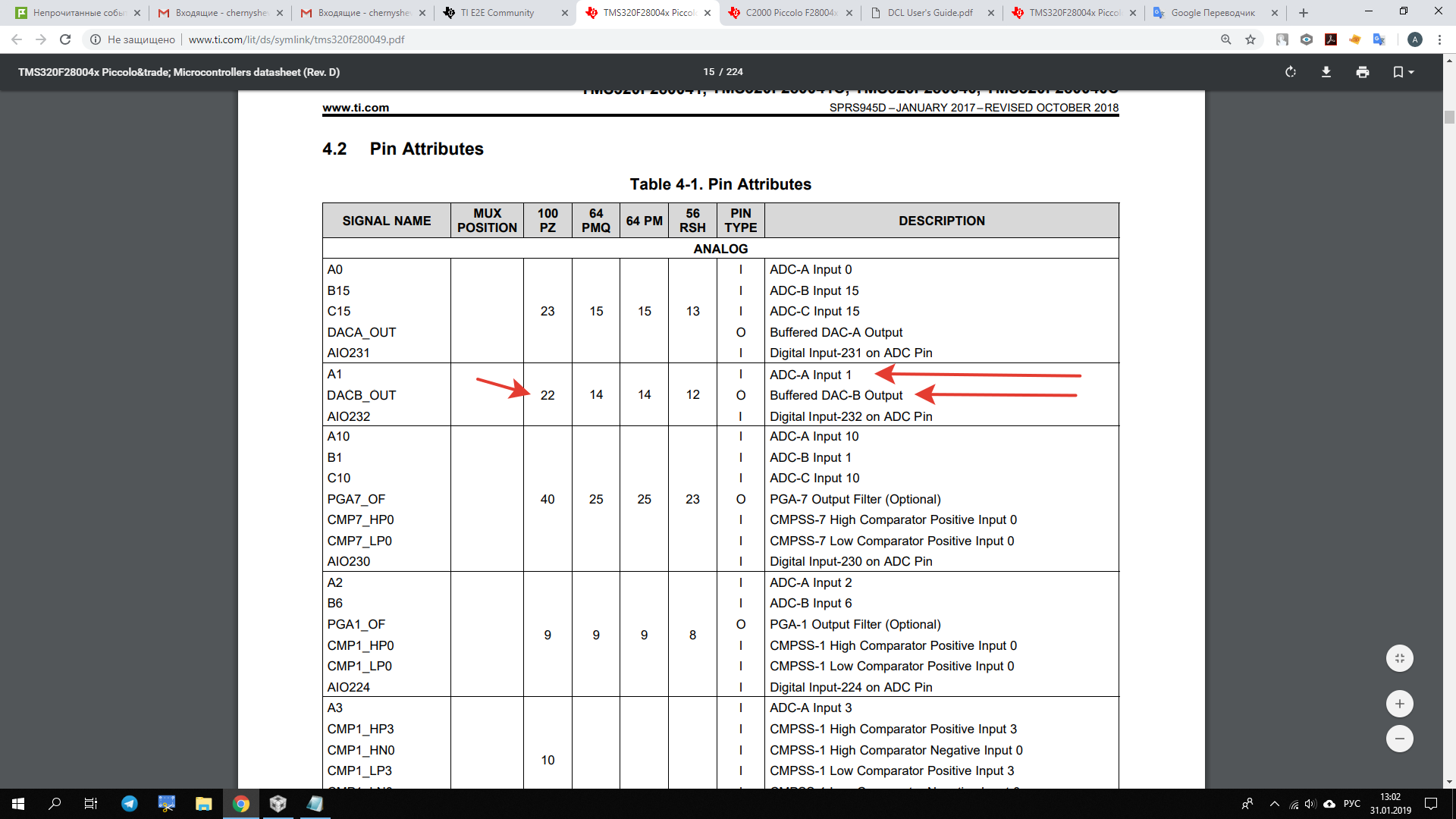
But for the rest of the pins that are not related to GPIO, I do not know how to choose the appropriate destination. For example, there is a pin 22 in the case of 100 pin (PZ). It has 3 functions: ADC-A Input 1, Buffered DAC-B Output, and Digital Input-232 on ADC Pin. Do I have to specify in what register what purpose of this pin I choose, since they cannot work together exactly (ADC and DAC). For this pin I launched DAC, it works fine. But if I also try to run the ADC, will there be any conflict?

And the most interesting question for me:
for example pin 10. It can be: CMPSS-1 High Comparator Positive Input 3, CMPSS-1 High Comparator Negative Input 0, CMPSS-1 Low Comparator Positive Input 3, CMPSS-1 Low Comparator Negative Input 0. How do I tell the CMPSS module, I want to use this pin exactly as CMPSS-1 High Comparator Negative Input 0? And how to inform the CMPSS module that it should work exactly with input 0?

  • Hi Andrey,

    When the pin you are using is purely a GPIO, then yes you are correct.  You have to program registers to ensure that the proper multiplex position will correspond to the pin function.  You can also dictate with the GPIO direction register whether the pin will act as an input or an output and you also configure some other attributes like turning on the pull up resistance or enable open drain capability if this was an output pin.  All these (and some other functions), you can do when dealing with pure GPIO pins.  These are the pins In table 4-1 (Pin attributes) of the device specification starting at below section (first pin is GPIO0, GPIO1...and so forth):

    At the start of table 4-1, the pins are categorized as analog pins, and these are the ones you have described in your post above.  Analog pins are the ports/interfaces that go directly to the analog modules which could be ADC, DAC, Comparator and PGA.  There are several instances of these analog modules within the F280049 device and all of these modules have direct connections to the analog pins.  Some analog pins have multiple connections to different modules, for example, as what you have highlighted above, pin 22 goes to ADC module A channel 1, as DAC module B output and as AIO232.  Pin 10 goes to ADC module A channel 3, Comparator module 1 high side  positive input 3, Comparator module 1 high side negative input 0, Comparator module 1 low side  positive input 3, Comparator module 1 low side negative input 0, and AIO233.  

    In the case of the comparator subsystem (CMPSS), you control the behavior of the comparator with the COMPCTL register (specifically with fields COMPLSOURCE and COMPHSOURCE).  The connections to the comparator inputs are controlled through registers CMPHPMXSEL, CMPLPMXSEL, CMPHNMXSEL, and CMPLNMXSEL.

    In the case of ADC, you still have to configure the channel source using ADCSOCxCTL (field CHSEL) as to which channel to convert even if the ADC inputs have direct connections to external pins and with DAC, output will be available on the DAC out pin as long as the DAC is enabled (using the DAC registers).  In the case of pin 22, DAC output B will always be connected to ADC module A input 1.  You can use the functionality of this pin to monitor DAC output B through ADC A channel 1 without configuring any registers.

    Also note that with the analog pins, another flexible function for these is for them to be used as GPIO pins but are fixed as INPUT only.  These are designated as AIOs from the table.  All AIOs are mapped to GPIO port H (GPIO224-GPIO247).

    A better way to understand these internal connections is to check Table 12-1 (Analog Pins and Internal Connections) of the F280049 Technical Reference Manual (SPRUI33A).  Table describes which analog channels have direct connections to analog modules (no register required to establish connection) and some that require mux connection through register configuration like the case of CMPSS.

    Hope this helps.

    Regards,

    Joseph

  • Joseph Casuga, thanks for the detailed answer! This in many ways clarified for me the understanding of the scheme of interaction and connection of analog channels.

    Thanks again!