


Part Number: TMS320F28377D
Hi there,
My transmit data from the TMS320 (spi slave) is delayed by one clock cycle and I'm not sure how to change this. The data I intend to send is loaded in SpicRegs.SPITXBUF like below. Here, PACKET_SIZE = 8 and
SPI_Data.txdata is an array corresponding to the highlighted memory at 0xA508. The data there is SPI_DATA.txdata = {0x43, 0x10, 0x08, 0x00, 0x20, 0x00, 0x00, 0x00}. One thing that the first figure below shows is that prior to entering the for loop, TXFFST is zero.
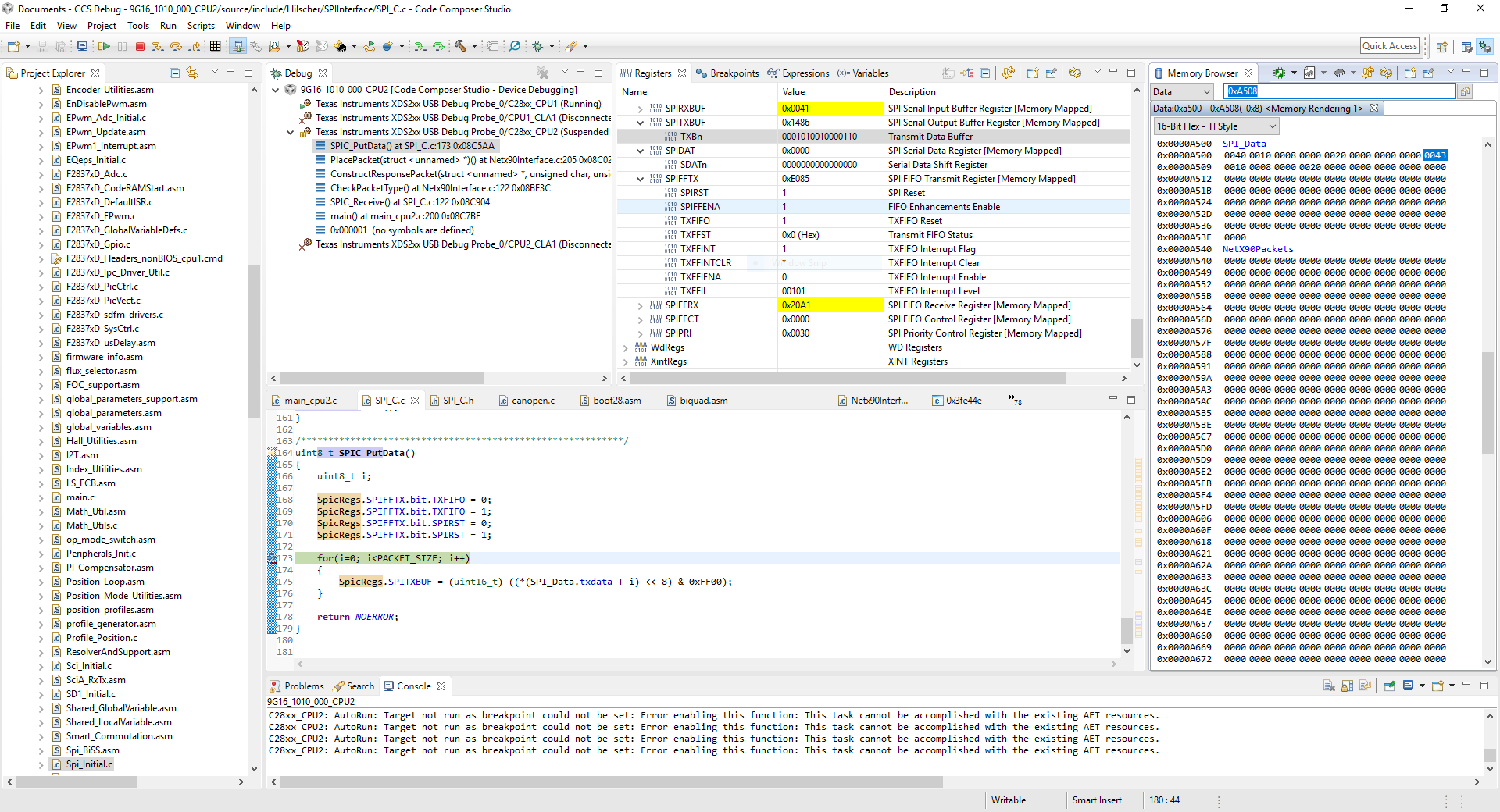
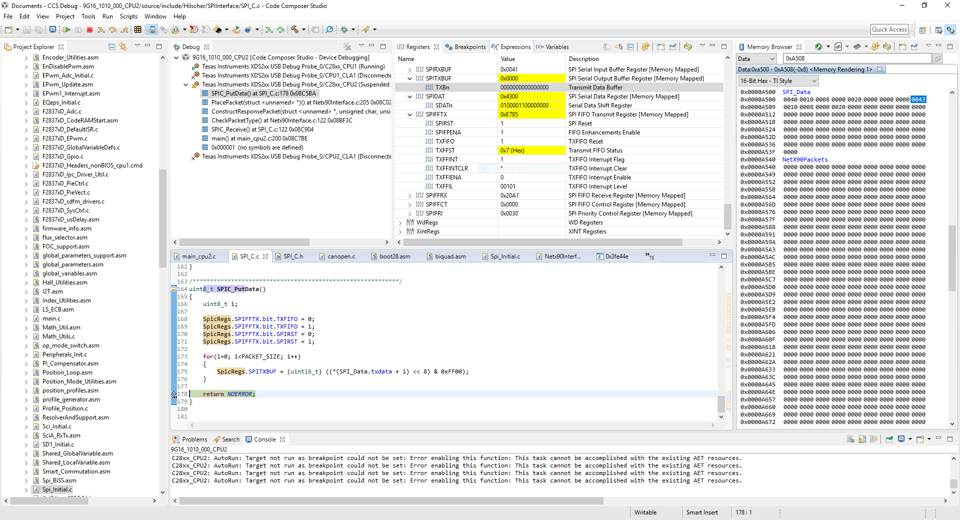
After exiting the for loop the first element in SPI_DATA.txdata was put into SPIDAT and the remaining elements get loaded into TXFFST causing TXFFST to be 7. SPIDAT reflects the value I expect- 0x4300 = 0x43 <<8. Based on this, I would think that I'm loading my data into the transmit FIFO correctly.
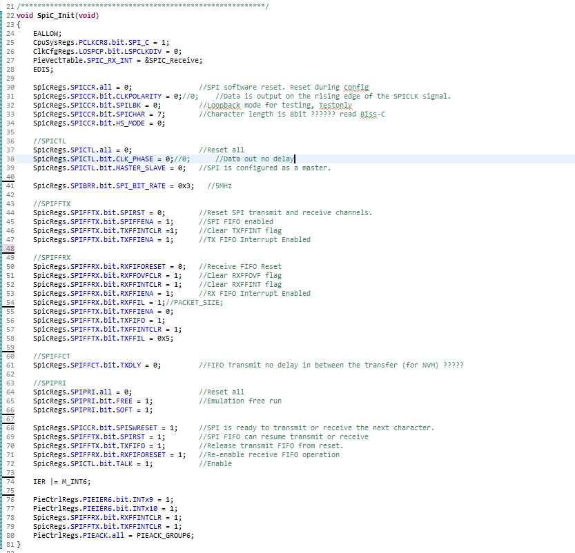
Here is how I initialize the *** registers. I would think the relevant thing is setting SPICCR.bit.CLKPOLARITY=0 AND SPICTL.bit.CLK_PHASE=0 if I want to operate in Mode 0 spi like my SPI Master.
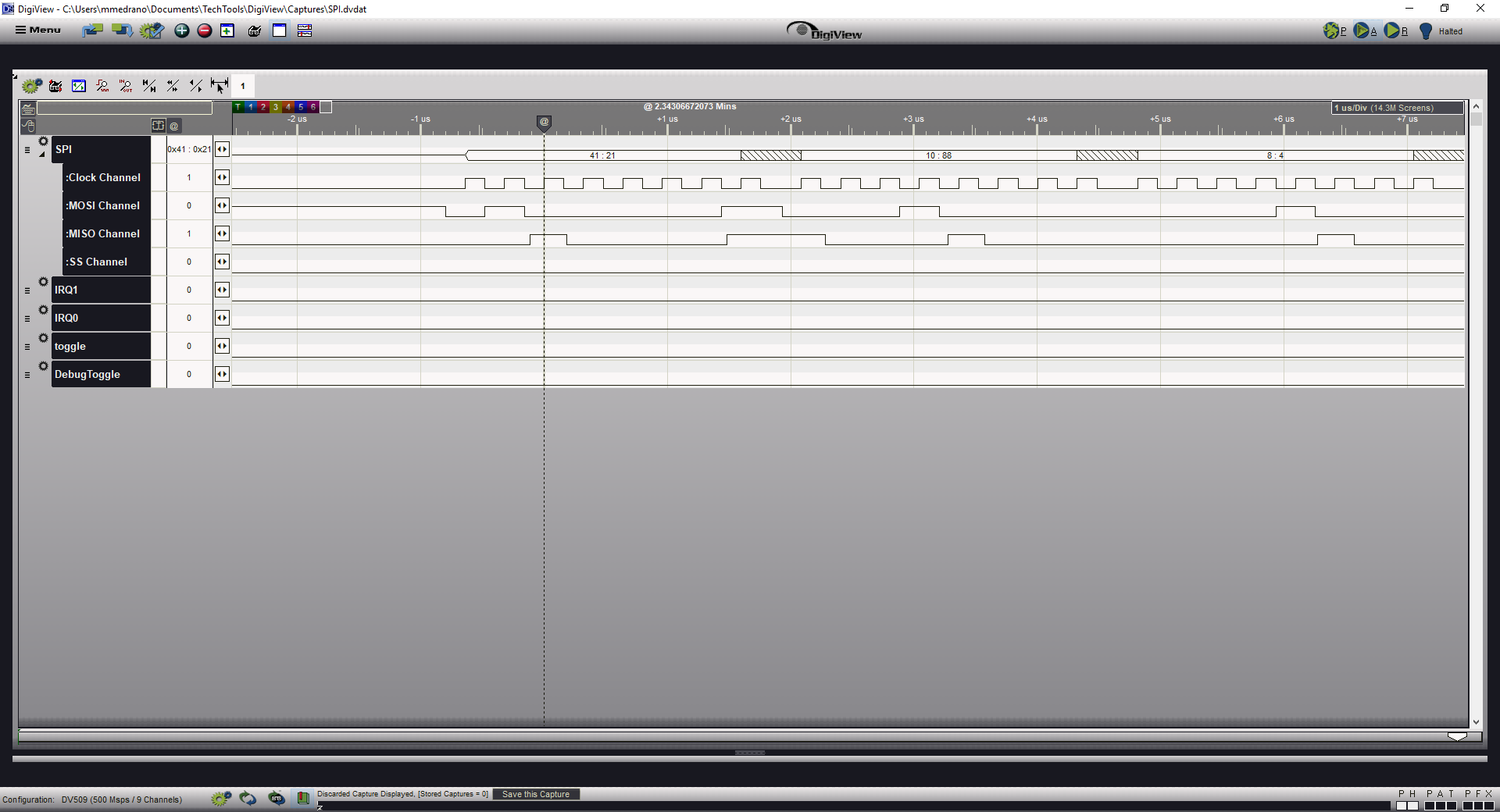
Here is a screenshot of the SPI signals from my logic analyzer (my SPI master agrees with the logic analyzer). The top of the figure shows 41:21, 10:88 and so on.. The left hand term represents the MOSI data from the SPI master and should be ignored. The right hand term shows 0x21, 0x88.. represents the MISO line - data output from my TMS320 spi slave.
I notice instead of clocking out the expected 0x4310080020000000 on the MISO line, the TMS320 clocks out 0x2188040010000000- which is the data I expect but delayed by one clock cycle. I've checked that the registers corresponding to the clock phase and clock polarity are set according to SPIC_init before and after a SPI transaction, but the TMS320 still sends its data in the wrong mode.
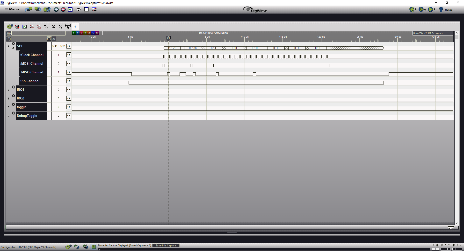
Here is a close up view of the first few bytes in the SPI transaction. Again the MISO line shows the data from the TMS320 SPI slave. The first byte clocked out is 0x21 instead of 0x43- which is what I would expect. All the MISO data just looks likes its delayed by one clock cycle. What am I doing wrong here?
Best,
Mike
