This thread has been locked.
If you have a related question, please click the "Ask a related question" button in the top right corner. The newly created question will be automatically linked to this question.
Team,
My customer has had his PWM modules linked together with the SYNC output of PWM1 provided to PWM2 – PWM6 through the master/slave PWM module configuration options. He is trying to break the link between modules 2 & 3 so that he can have the following daisy chains:
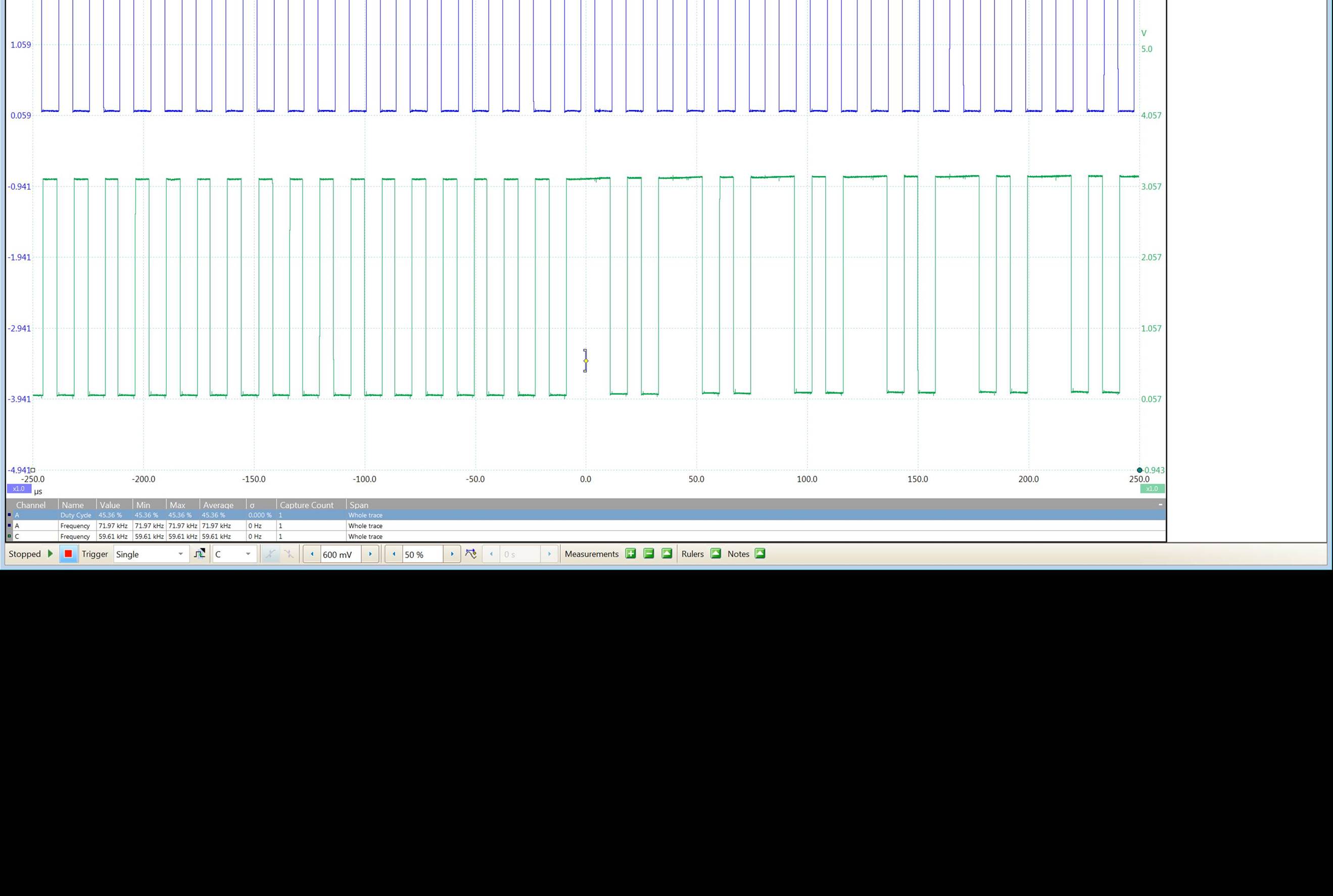
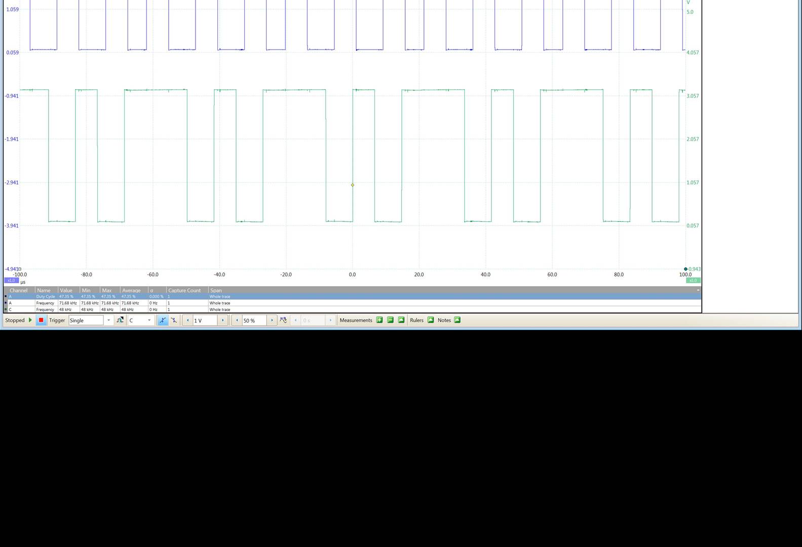
When customer tried setting EPwm3Regs.TBCTL.bit.PHSEN = TB_DISABLE he found that the CTR would pause at one count for a period of time on both the count up and count down. This is all using Matlab Simulink auto-generated code that is pulling in a custom C module to help with the configuration of the PWM. The PWM is also triggering an ISR that is used for calculation of all of the control code. There is some issue with the way that it is configured that is preventing him from achieving good operation when he does not link all the PWMs as a slave to PWM1.
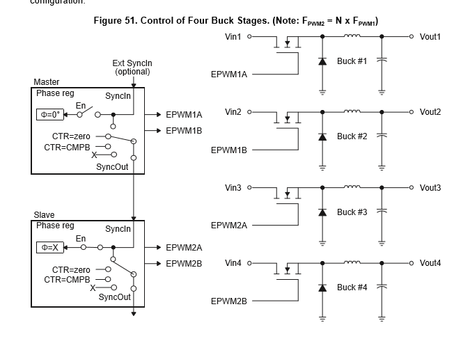
See figure 51 - here: http://www.ti.com/lit/ug/sprug04a/sprug04a.pdf
Your inputs would be greatly appreciated.
Thanks!
Viktorija
Viktorija,
There should be no issue with separating the ePWM sync chain into two time domains.
Can you provide more details here?Viktorija Cecil said:he found that the CTR would pause at one count for a period of time on both the count up and count down.
Brian McKay have you seen any issues similar to this when using ePWM sync chain?
Regards,
Cody
Cody,
Here are details from customer:
I finally was able to reproduce a problem(s) that we need to resolve with the PWM modulators written with purely C code. There are two problems that I can replicate in C code, as well as model-based. I apologize for the length of this e-mail, but it is very important to communicate the issue(s) so that they can be understood and addressed.
First, our objective is to have:
Here’s how I have setup the PWM modulators:
Active Front End (ePWM1 and ePWM2):
Here is my code for initialization of ePWM1 and ePWM2 to achieve the above results:
void EPwm1Init(void)
{
/*** Initialize ePWM1 modules ***/
/*-- Setup Time-Base (TB) Submodule --*/
EPwm1Regs.TBPRD = PLL_FREQUENCY / AfePwmFrequency * 0.5; // Multiply by 0.5 because we're using an up/down counter and the period is half the frequency
// Time-Base Control Register
EPwm1Regs.TBCTL.bit.CTRMODE = TB_COUNT_UPDOWN; // Counter Mode
EPwm1Regs.TBCTL.bit.SYNCOSEL = TB_CTR_ZERO; // Sync output select to downstream ePWM2 module
EPwm1Regs.TBCTL.bit.PRDLD = TB_SHADOW; // Shadow select
EPwm1Regs.TBCTL.bit.PHSEN = TB_ENABLE; // Phase load enable
EPwm1Regs.TBCTL.bit.PHSDIR = TB_DOWN; // Phase Direction
EPwm1Regs.TBCTL.bit.HSPCLKDIV = TB_DIV1; // High speed time pre-scale
EPwm1Regs.TBCTL.bit.CLKDIV = TB_DIV1; // Timebase clock pre-scale
// Time-Base Phase Register
EPwm1Regs.TBPHS.half.TBPHS = 0; // Phase offset register
EPwm1Regs.TBCTR = 0x0000; /* Clear counter*/
/*-- Setup Counter_Compare (CC) Submodule --*/
// Counter-Compare Control Register
EPwm1Regs.CMPCTL.bit.SHDWAMODE = CC_SHADOW; // Compare A block operating mode.
EPwm1Regs.CMPCTL.bit.SHDWBMODE = CC_SHADOW; // Compare B block operating mode.
EPwm1Regs.CMPCTL.bit.LOADAMODE = CC_CTR_ZERO_PRD; // Active compare A
EPwm1Regs.CMPCTL.bit.LOADBMODE = CC_CTR_ZERO_PRD; // Active compare A
EPwm1Regs.CMPA.half.CMPA = EPwm1Regs.TBPRD * 0.5; // 50% modulation
EPwm1Regs.CMPB = EPwm1Regs.TBPRD * 0.5; // 50% modulation
/*-- Setup Action-Qualifier (AQ) Submodule --*/
EPwm1Regs.AQCTLA.bit.CAU = AQ_CLEAR; // Clear PWM when latch value = counter when counting up
EPwm1Regs.AQCTLA.bit.CAD = AQ_SET; // Set PWM when latch value = counter when counting down
EPwm1Regs.AQCTLA.bit.ZRO = AQ_NO_ACTION; // No action PWM when counter = 0
EPwm1Regs.AQCTLA.bit.PRD = AQ_NO_ACTION; // Do nothing when counter = period
EPwm1Regs.AQCTLA.bit.CBU = AQ_NO_ACTION; // Do nothing when latch value = counter when counting up
EPwm1Regs.AQCTLA.bit.CBD = AQ_NO_ACTION; // Do nothing when latch value = counter when counting down
/* Setup action qualifiers for B module */
EPwm1Regs.AQCTLB.bit.CAU = AQ_SET; // Set PWM when latch value = counter when counting up
EPwm1Regs.AQCTLB.bit.CAD = AQ_CLEAR; // Clear when latch value = counter when counting down
EPwm1Regs.AQCTLB.bit.ZRO = AQ_NO_ACTION; // Do nothing PWM when latch counter = 0
EPwm1Regs.AQCTLB.bit.PRD = AQ_NO_ACTION; // Do nothing when counter = period
EPwm1Regs.AQCTLB.bit.CBU = AQ_NO_ACTION; // Do nothing when counter = latch value when counting up on B sub-module
EPwm1Regs.AQCTLB.bit.CBD = AQ_NO_ACTION; // Do nothing when counter = latch value when counting down on B sub-module
// Action-Qualifier Software Force Register
EPwm1Regs.AQSFRC.bit.RLDCSF = 3; // Reload from Shadow options
// Action-Qualifier Continuous S/W Force Register Set
EPwm1Regs.AQCSFRC.bit.CSFA = 0; // Continuous Software Force on output A
EPwm1Regs.AQCSFRC.bit.CSFB = 0; // Continuous Software Force on output B
/*-- Setup Dead-Band Generator (DB) Submodule --*/
// Dead-Band Generator Control Register
EPwm1Regs.DBCTL.bit.OUT_MODE = 3; // Dead Band Output Mode Control
EPwm1Regs.DBCTL.bit.IN_MODE = 0; // Dead Band Input Select Mode Control
EPwm1Regs.DBCTL.bit.POLSEL = 2; // Polarity Select Control
EPwm1Regs.DBRED = (Uint16)(PLL_FREQUENCY * AfeDeadtime);
EPwm1Regs.DBFED = (Uint16)(PLL_FREQUENCY * AfeDeadtime);
/*-- Setup Event-Trigger (ET) Submodule --*/
// Event-Trigger Selection and Event-Trigger Pre-Scale Register
EPwm1Regs.ETSEL.bit.SOCAEN = 1; // Start of conversion A Enable
EPwm1Regs.ETSEL.bit.SOCASEL = 1; // Start of conversion A Select
EPwm1Regs.ETPS.bit.SOCAPRD = 2; // EPWM1SOCA Period Select
EPwm1Regs.ETSEL.bit.SOCBEN = 0; // Start of conversion B Enable
EPwm1Regs.ETSEL.bit.SOCBSEL = 1; // Start of conversion B Select
EPwm1Regs.ETPS.bit.SOCBPRD = 1; // EPWM1SOCB Period Select
EPwm1Regs.ETSEL.bit.INTEN = 1; // EPWM1INTn Enable
EPwm1Regs.ETSEL.bit.INTSEL = ET_CTR_PRD; // EPWM1INTn Select
EPwm1Regs.ETPS.bit.INTPRD = ET_3RD; // EPWM1INTn Period Select
/*-- Setup PWM-Chopper (PC) Submodule --*/
// PWM-Chopper Control Register
EPwm1Regs.PCCTL.bit.CHPEN = 0; // PWM chopping enable
EPwm1Regs.PCCTL.bit.CHPFREQ = 0; // Chopping clock frequency
EPwm1Regs.PCCTL.bit.OSHTWTH = 0; // One-shot pulse width
EPwm1Regs.PCCTL.bit.CHPDUTY = 0; // Chopping clock Duty cycle
/*-- Set up Trip-Zone (TZ) Submodule --*/
EALLOW;
EPwm1Regs.TZSEL.all = 0;
// Trip-Zone Control Register
EPwm1Regs.TZCTL.bit.TZA = 2; // TZ1 to TZ6 Trip Action On EPWM1A
EPwm1Regs.TZCTL.bit.TZB = 2; // TZ1 to TZ6 Trip Action On EPWM1B
// Trip-Zone Enable Interrupt Register
EPwm1Regs.TZEINT.bit.OST = 0; // Trip Zones One Shot Int Enable
EPwm1Regs.TZEINT.bit.CBC = 0; // Trip Zones Cycle By Cycle Int Enable
EDIS;
} /* End of EPwm1Init */
void EPwm2Init(void)
{
/*** Initialize ePWM2 modules ***/
/*-- Setup Time-Base (TB) Submodule --*/
EPwm2Regs.TBPRD = PLL_FREQUENCY / AfePwmFrequency * 0.5; // Multiply by 0.5 because we're using an up/down counter and the period is half the frequency
// Time-Base Control Register
EPwm2Regs.TBCTL.bit.CTRMODE = TB_COUNT_UPDOWN; // Counter Mode
EPwm2Regs.TBCTL.bit.SYNCOSEL = TB_DISABLE; // NO downstream synchronization to ePWM3 module
EPwm2Regs.TBCTL.bit.PRDLD = TB_SHADOW; // Shadow select
EPwm2Regs.TBCTL.bit.PHSEN = TB_ENABLE; // Phase load enable
EPwm2Regs.TBCTL.bit.PHSDIR = TB_DOWN; // Phase Direction
EPwm2Regs.TBCTL.bit.HSPCLKDIV = TB_DIV1; // High speed time pre-scale
EPwm2Regs.TBCTL.bit.CLKDIV = TB_DIV1; // Timebase clock pre-scale
// Time-Base Phase Register
EPwm2Regs.TBPHS.half.TBPHS = 0; // Phase offset register
EPwm2Regs.TBCTR = 0x0000; /* Clear counter*/
/*-- Setup Counter_Compare (CC) Submodule --*/
// Counter-Compare Control Register
EPwm2Regs.CMPCTL.bit.SHDWAMODE = CC_SHADOW; // Compare A block operating mode.
EPwm2Regs.CMPCTL.bit.SHDWBMODE = CC_SHADOW; // Compare B block operating mode.
EPwm2Regs.CMPCTL.bit.LOADAMODE = CC_CTR_ZERO_PRD; // Active compare A
EPwm2Regs.CMPCTL.bit.LOADBMODE = CC_CTR_ZERO_PRD; // Active compare A
EPwm2Regs.CMPA.half.CMPA = (Uint16)(EPwm2Regs.TBPRD * 0.5); // Startup with 50% modulation
EPwm2Regs.CMPB = (Uint16)(EPwm2Regs.TBPRD * 0.5); // Startup with 50% modulation
/*-- Setup Action-Qualifier (AQ) Submodule --*/
EPwm2Regs.AQCTLA.bit.CAU = AQ_CLEAR; // Clear PWM when latch value = counter when counting up
EPwm2Regs.AQCTLA.bit.CAD = AQ_SET; // Set PWM when latch value = counter when counting down
EPwm2Regs.AQCTLA.bit.ZRO = AQ_NO_ACTION; // No action PWM when counter = 0
EPwm2Regs.AQCTLA.bit.PRD = AQ_NO_ACTION; // Do nothing when counter = period
EPwm2Regs.AQCTLA.bit.CBU = AQ_NO_ACTION; // Do nothing when latch value = counter when counting up
EPwm2Regs.AQCTLA.bit.CBD = AQ_NO_ACTION; // Do nothing when latch value = counter when counting down
/* Setup action qualifiers for B module */
EPwm2Regs.AQCTLB.bit.CAU = AQ_SET; // Set PWM when latch value = counter when counting up
EPwm2Regs.AQCTLB.bit.CAD = AQ_CLEAR; // Clear when latch value = counter when counting down
EPwm2Regs.AQCTLB.bit.ZRO = AQ_NO_ACTION; // Do nothing PWM when latch counter = 0
EPwm2Regs.AQCTLB.bit.PRD = AQ_NO_ACTION; // Do nothing when counter = period
EPwm2Regs.AQCTLB.bit.CBU = AQ_NO_ACTION; // Do nothing when counter = latch value when counting up on B sub-module
EPwm2Regs.AQCTLB.bit.CBD = AQ_NO_ACTION; // Do nothing when counter = latch value when counting down on B sub-module
// Action-Qualifier Software Force Register
EPwm2Regs.AQSFRC.bit.RLDCSF = 3; // Reload from Shadow options
// Action-Qualifier Continuous S/W Force Register Set
EPwm2Regs.AQCSFRC.bit.CSFA = 0; // Continuous Software Force on output A
EPwm2Regs.AQCSFRC.bit.CSFB = 0; // Continuous Software Force on output B
/*-- Setup Dead-Band Generator (DB) Submodule --*/
// Dead-Band Generator Control Register
EPwm2Regs.DBCTL.bit.OUT_MODE = 3; // Dead Band Output Mode Control
EPwm2Regs.DBCTL.bit.IN_MODE = 0; // Dead Band Input Select Mode Control
EPwm2Regs.DBCTL.bit.POLSEL = 2; // Polarity Select Control
EPwm2Regs.DBRED = (Uint16)(PLL_FREQUENCY * AfeDeadtime);
EPwm2Regs.DBFED = (Uint16)(PLL_FREQUENCY * AfeDeadtime);
/*-- Setup Event-Trigger (ET) Submodule --*/
// Event-Trigger Selection and Event-Trigger Pre-Scale Register
EPwm2Regs.ETSEL.bit.SOCAEN = 0; // Start of conversion A Enable
EPwm2Regs.ETSEL.bit.SOCASEL = 1; // Start of conversion A Select
EPwm2Regs.ETPS.bit.SOCAPRD = 3; // EPWM2SOCA Period Select
EPwm2Regs.ETSEL.bit.SOCBEN = 0; // Start of conversion B Enable
EPwm2Regs.ETSEL.bit.SOCBSEL = 1; // Start of conversion B Select
EPwm2Regs.ETPS.bit.SOCBPRD = 1; // EPWM2SOCB Period Select
EPwm2Regs.ETSEL.bit.INTEN = 0; // EPWM2INTn Enable
EPwm2Regs.ETSEL.bit.INTSEL = 2; // EPWM2INTn Select
EPwm2Regs.ETPS.bit.INTPRD = 3; // EPWM2INTn Period Select
/*-- Setup PWM-Chopper (PC) Submodule --*/
// PWM-Chopper Control Register
EPwm2Regs.PCCTL.bit.CHPEN = 0; // PWM chopping enable
EPwm2Regs.PCCTL.bit.CHPFREQ = 0; // Chopping clock frequency
EPwm2Regs.PCCTL.bit.OSHTWTH = 0; // One-shot pulse width
EPwm2Regs.PCCTL.bit.CHPDUTY = 0; // Chopping clock Duty cycle
/*-- Set up Trip-Zone (TZ) Submodule --*/
EALLOW;
EPwm2Regs.TZSEL.all = 0;
// Trip-Zone Control Register
EPwm2Regs.TZCTL.bit.TZA = 2; // TZ1 to TZ6 Trip Action On EPWM2A
EPwm2Regs.TZCTL.bit.TZB = 2; // TZ1 to TZ6 Trip Action On EPWM2B
// Trip-Zone Enable Interrupt Register
EPwm2Regs.TZEINT.bit.OST = 0; // Trip Zones One Shot Int Enable
EPwm2Regs.TZEINT.bit.CBC = 0; // Trip Zones Cycle By Cycle Int Enable
EDIS;
} /* End of EPwm2Init */
NOTE that EPwm2Regs.TBCTL.bit.SYNCOSEL = TB_DISABLE; This should disable downstream synchronization with module ePWM3
ePWM3 and ePWM4 are initialized with the following code to achieve the above defined objectives:
void EPwm3Init(void)
{
/*** Initialize ePWM3 modules ***/
/*-- Setup Time-Base (TB) Submodule --*/
EPwm3Regs.TBPRD = (Uint32)(PLL_FREQUENCY / DabPwmFrequency * 0.5); // Multiply by 0.5 because we're using an up/down counter and the period is half the frequency
// Time-Base Control Register
EPwm3Regs.TBCTL.bit.CTRMODE = TB_COUNT_UPDOWN; // Counter Mode
EPwm3Regs.TBCTL.bit.SYNCOSEL = TB_CTR_ZERO; // Synchronize downstream modules
EPwm3Regs.TBCTL.bit.PRDLD = TB_SHADOW; // Shadow select
EPwm3Regs.TBCTL.bit.PHSEN = TB_ENABLE; // Phase load enable
EPwm3Regs.TBCTL.bit.PHSDIR = TB_DOWN; // Phase Direction
EPwm3Regs.TBCTL.bit.HSPCLKDIV = TB_DIV1; // High speed time pre-scale
EPwm3Regs.TBCTL.bit.CLKDIV = TB_DIV1; // Timebase clock pre-scale
// Time-Base Phase Register
EPwm3Regs.TBPHS.half.TBPHS = 0; // Phase offset register
EPwm3Regs.TBCTR = 0x0000; /* Clear counter*/
/*-- Setup Counter_Compare (CC) Submodule --*/
// Counter-Compare Control Register
EPwm3Regs.CMPCTL.bit.SHDWAMODE = 0; // Compare A block operating mode.
EPwm3Regs.CMPCTL.bit.SHDWBMODE = 0; // Compare B block operating mode.
EPwm3Regs.CMPCTL.bit.LOADAMODE = 0; // Active compare A
EPwm3Regs.CMPCTL.bit.LOADBMODE = 0; // Active compare A
EPwm3Regs.CMPA.half.CMPA = (Uint16)(EPwm3Regs.TBPRD * 0.5); // 50% duty cycle -- no longer matters due to setting of AQCTLA.bit.ZRO and .PRD action qualifiers
EPwm3Regs.CMPB = (Uint16)(EPwm3Regs.TBPRD * 0.5); // 50% duty cycle -- no longer matters due to setting of AQCTLA.bit.ZRO and .PRD action qualifiers
/*-- Setup Action-Qualifier (AQ) Submodule --*/
/* Setup action qualifiers for A module */
EPwm3Regs.AQCTLA.bit.CAU = AQ_NO_ACTION; // Do nothing when latch value = counter when counting up
EPwm3Regs.AQCTLA.bit.CAD = AQ_NO_ACTION; // Do nothing when latch value = counter when counting down
EPwm3Regs.AQCTLA.bit.ZRO = AQ_SET; // Set PWM when counter = 0
EPwm3Regs.AQCTLA.bit.PRD = AQ_CLEAR; // Clear when counter = period
EPwm3Regs.AQCTLA.bit.CBU = AQ_NO_ACTION; // Do nothing when latch value = counter when counting up
EPwm3Regs.AQCTLA.bit.CBD = AQ_NO_ACTION; // Do nothing when latch value = counter when counting down
/* Setup action qualifiers for B module */
EPwm3Regs.AQCTLB.bit.CAU = AQ_NO_ACTION; // Do nothing when latch value = counter when counting up
EPwm3Regs.AQCTLB.bit.CAD = AQ_NO_ACTION; // Do nothing when latch value = counter when counting down
EPwm3Regs.AQCTLB.bit.ZRO = AQ_CLEAR; // Clear PWM when latch counter = 0
EPwm3Regs.AQCTLB.bit.PRD = AQ_SET; // Set when counter = period
EPwm3Regs.AQCTLB.bit.CBU = AQ_NO_ACTION; // Do nothing when counter = latch value when counting up on B sub-module
EPwm3Regs.AQCTLB.bit.CBD = AQ_NO_ACTION; // Do nothing when counter = latch value when counting down on B sub-module
// Action-Qualifier Software Force Register
EPwm3Regs.AQSFRC.bit.RLDCSF = 3; // Reload from Shadow options
// Action-Qualifier Continuous S/W Force Register Set
EPwm3Regs.AQCSFRC.bit.CSFA = 0; // Continuous Software Force on output A
EPwm3Regs.AQCSFRC.bit.CSFB = 0; // Continuous Software Force on output B
/*-- Setup Dead-Band Generator (DB) Submodule --*/
// Dead-Band Generator Control Register
EPwm3Regs.DBCTL.bit.OUT_MODE = 3; // Dead Band Output Mode Control
EPwm3Regs.DBCTL.bit.IN_MODE = 0; // Dead Band Input Select Mode Control
EPwm3Regs.DBCTL.bit.POLSEL = 2; // Polarity Select Control
// EPwm3Regs.DBCTL.all = (EPwm3Regs.DBCTL.all & ~0x3F) | 0xB;
EPwm3Regs.DBRED = (Uint16)(PLL_FREQUENCY * DabDeadtime);
EPwm3Regs.DBFED = (Uint16)(PLL_FREQUENCY * DabDeadtime);
/*-- Setup Event-Trigger (ET) Submodule --*/
// Event-Trigger Selection and Event-Trigger Pre-Scale Register
EPwm3Regs.ETSEL.bit.SOCAEN = 0; // Start of conversion A Enable
EPwm3Regs.ETSEL.bit.SOCASEL = 1; // Start of conversion A Select
EPwm3Regs.ETPS.bit.SOCAPRD = 3; // EPWM3SOCA Period Select
EPwm3Regs.ETSEL.bit.SOCBEN = 0; // Start of conversion B Enable
EPwm3Regs.ETSEL.bit.SOCBSEL = 1; // Start of conversion B Select
EPwm3Regs.ETPS.bit.SOCBPRD = 1; // EPWM3SOCB Period Select
EPwm3Regs.ETSEL.bit.INTEN = 0; // EPWM3INTn Enable
EPwm3Regs.ETSEL.bit.INTSEL = 1; // EPWM3INTn Select
EPwm3Regs.ETPS.bit.INTPRD = 3; // EPWM3INTn Period Select
/*-- Setup PWM-Chopper (PC) Submodule --*/
// PWM-Chopper Control Register
EPwm3Regs.PCCTL.bit.CHPEN = 0; // PWM chopping enable
EPwm3Regs.PCCTL.bit.CHPFREQ = 0; // Chopping clock frequency
EPwm3Regs.PCCTL.bit.OSHTWTH = 0; // One-shot pulse width
EPwm3Regs.PCCTL.bit.CHPDUTY = 0; // Chopping clock Duty cycle
/*-- Set up Trip-Zone (TZ) Submodule --*/
EALLOW;
EPwm3Regs.TZSEL.all = 0;
// Trip-Zone Control Register
EPwm3Regs.TZCTL.bit.TZA = 2; // TZ1 to TZ6 Trip Action On EPWM3A
EPwm3Regs.TZCTL.bit.TZB = 2; // TZ1 to TZ6 Trip Action On EPWM3B
// Trip-Zone Enable Interrupt Register
EPwm3Regs.TZEINT.bit.OST = 0; // Trip Zones One Shot Int Enable
EPwm3Regs.TZEINT.bit.CBC = 0; // Trip Zones Cycle By Cycle Int Enable
EDIS;
} /* End of EPwm3Init */
void EPwm4Init(void)
{
/*** Initialize ePWM4 modules ***/
/*-- Setup Time-Base (TB) Submodule --*/
EPwm4Regs.TBPRD = PLL_FREQUENCY / DabPwmFrequency * 0.5; // Multiply by 0.5 because we're using an up/down counter and the period is half the frequency
// Time-Base Control Register
EPwm4Regs.TBCTL.bit.CTRMODE = TB_COUNT_UPDOWN; // Counter Mode
EPwm4Regs.TBCTL.bit.SYNCOSEL = TB_SYNC_IN; // Synchronize downstream module ePWM5
EPwm4Regs.TBCTL.bit.PRDLD = TB_SHADOW; // Shadow select
EPwm4Regs.TBCTL.bit.PHSEN = TB_ENABLE; // Phase load enable
EPwm4Regs.TBCTL.bit.PHSDIR = TB_DOWN; // Phase Direction
EPwm4Regs.TBCTL.bit.HSPCLKDIV = TB_DIV1; // High speed time pre-scale
EPwm4Regs.TBCTL.bit.CLKDIV = TB_DIV1; // Timebase clock pre-scale
// EPwm4Regs.TBCTL.all = (EPwm4Regs.TBCTL.all & ~0x3FBF) | 0x484;
// Time-Base Phase Register
EPwm4Regs.TBPHS.half.TBPHS = 0; // Phase offset register
EPwm4Regs.TBCTR = 0x0000; /* Clear counter*/
/*-- Setup Counter_Compare (CC) Submodule --*/
// Counter-Compare Control Register
EPwm4Regs.CMPCTL.bit.SHDWAMODE = 0; // Compare A block operating mode.
EPwm4Regs.CMPCTL.bit.SHDWBMODE = 0; // Compare B block operating mode.
EPwm4Regs.CMPCTL.bit.LOADAMODE = 0; // Active compare A
EPwm4Regs.CMPCTL.bit.LOADBMODE = 0; // Active compare A
EPwm4Regs.CMPA.half.CMPA = (Uint16)(EPwm4Regs.TBPRD * 0.5); // 50% duty cycle -- no longer matters due to setting of AQCTLA.bit.ZRO and .PRD action qualifiers
EPwm4Regs.CMPB = (Uint16)(EPwm4Regs.TBPRD * 0.5); // 50% duty cycle -- no longer matters due to setting of AQCTLA.bit.ZRO and .PRD action qualifiers
/*-- Setup Action-Qualifier (AQ) Submodule --*/
/* Setup action qualifiers for A module */
EPwm4Regs.AQCTLA.bit.CAU = AQ_NO_ACTION; // Do nothing when latch value = counter when counting up
EPwm4Regs.AQCTLA.bit.CAD = AQ_NO_ACTION; // Do nothing when latch value = counter when counting down
EPwm4Regs.AQCTLA.bit.ZRO = AQ_CLEAR; // Clear PWM when counter = 0
EPwm4Regs.AQCTLA.bit.PRD = AQ_SET; // Set when counter = period
EPwm4Regs.AQCTLA.bit.CBU = AQ_NO_ACTION; // Do nothing when latch value = counter when counting up
EPwm4Regs.AQCTLA.bit.CBD = AQ_NO_ACTION; // Do nothing when latch value = counter when counting down
/* Setup action qualifiers for B module */
EPwm4Regs.AQCTLB.bit.CAU = AQ_NO_ACTION; // Do nothing when latch value = counter when counting up
EPwm4Regs.AQCTLB.bit.CAD = AQ_NO_ACTION; // Do nothing when latch value = counter when counting down
EPwm4Regs.AQCTLB.bit.ZRO = AQ_SET; // Set PWM when latch counter = 0
EPwm4Regs.AQCTLB.bit.PRD = AQ_CLEAR; // Clear when counter = period
EPwm4Regs.AQCTLB.bit.CBU = AQ_NO_ACTION; // Do nothing when counter = latch value when counting up on B sub-module
EPwm4Regs.AQCTLB.bit.CBD = AQ_NO_ACTION; // Do nothing when counter = latch value when counting down on B sub-module
// Action-Qualifier Software Force Register
EPwm4Regs.AQSFRC.bit.RLDCSF = 3; // Reload from Shadow options
// Action-Qualifier Continuous S/W Force Register Set
EPwm4Regs.AQCSFRC.bit.CSFA = 0; // Continuous Software Force on output A
EPwm4Regs.AQCSFRC.bit.CSFB = 0; // Continuous Software Force on output B
/*-- Setup Dead-Band Generator (DB) Submodule --*/
// Dead-Band Generator Control Register
EPwm4Regs.DBCTL.bit.OUT_MODE = 3; // Dead Band Output Mode Control
EPwm4Regs.DBCTL.bit.IN_MODE = 0; // Dead Band Input Select Mode Control
EPwm4Regs.DBCTL.bit.POLSEL = 2; // Polarity Select Control
EPwm4Regs.DBRED = (Uint16)(PLL_FREQUENCY * DabDeadtime);
EPwm4Regs.DBFED = (Uint16)(PLL_FREQUENCY * DabDeadtime);
/*-- Setup Event-Trigger (ET) Submodule --*/
// Event-Trigger Selection and Event-Trigger Pre-Scale Register
EPwm4Regs.ETSEL.bit.SOCAEN = 0; // Start of conversion A Enable
EPwm4Regs.ETSEL.bit.SOCASEL = 1; // Start of conversion A Select
EPwm4Regs.ETPS.bit.SOCAPRD = 3; // EPWM4SOCA Period Select
EPwm4Regs.ETSEL.bit.SOCBEN = 0; // Start of conversion B Enable
EPwm4Regs.ETSEL.bit.SOCBSEL = 1; // Start of conversion B Select
EPwm4Regs.ETPS.bit.SOCBPRD = 1; // EPWM4SOCB Period Select
EPwm4Regs.ETSEL.bit.INTEN = 0; // EPWM4INTn Enable
EPwm4Regs.ETSEL.bit.INTSEL = 1; // EPWM4INTn Select
EPwm4Regs.ETPS.bit.INTPRD = 1; // EPWM4INTn Period Select
/*-- Setup PWM-Chopper (PC) Submodule --*/
// PWM-Chopper Control Register
EPwm4Regs.PCCTL.bit.CHPEN = 0; // PWM chopping enable
EPwm4Regs.PCCTL.bit.CHPFREQ = 0; // Chopping clock frequency
EPwm4Regs.PCCTL.bit.OSHTWTH = 0; // One-shot pulse width
EPwm4Regs.PCCTL.bit.CHPDUTY = 0; // Chopping clock Duty cycle
/*-- Set up Trip-Zone (TZ) Submodule --*/
EALLOW;
EPwm4Regs.TZSEL.all = 0;
// Trip-Zone Control Register
EPwm4Regs.TZCTL.bit.TZA = 2; // TZ1 to TZ6 Trip Action On EPWM4A
EPwm4Regs.TZCTL.bit.TZB = 2; // TZ1 to TZ6 Trip Action On EPWM4B
// Trip-Zone Enable Interrupt Register
EPwm4Regs.TZEINT.bit.OST = 0; // Trip Zones One Shot Int Enable
EPwm4Regs.TZEINT.bit.CBC = 0; // Trip Zones Cycle By Cycle Int Enable
EDIS;
} /* End of EPwm4Init */
NOTE that EPwm3Regs.TBCTL.bit.SYNCOSEL = TB_CTR_ZERO; This should initiate a downstream synchronization pulse when the counter = 0, thus having the effect of synchronizing the time-bases and phase changes for EPwm4, 5 and 6 with EPwm3, as long as EPwmNRegs.TBCTL.bit.SYNCOSEL = TB_SYNC_IN, where N = 4, 5 and 6.
Finally, ePWM5 and ePWM6 must be initialized to be 180 degrees out of phase with ePWM3 and ePWM4, but also allow for continuous phase changes during operation to control current. This is accomplished with the following code to initialize ePWM 5 and ePWM6:
void EPwm5Init(void)
{
/*** Initialize ePWM5 modules ***/
/*-- Setup Time-Base (TB) Submodule --*/
EPwm5Regs.TBPRD = PLL_FREQUENCY / DabPwmFrequency * 0.5; // Multiply by 0.5 because we're using an up/down counter and the period is half the frequency
// Time-Base Control Register
EPwm5Regs.TBCTL.bit.CTRMODE = TB_COUNT_UPDOWN; // Counter Mode
EPwm5Regs.TBCTL.bit.SYNCOSEL = TB_SYNC_IN; // Sync output select
EPwm5Regs.TBCTL.bit.PRDLD = TB_SHADOW; // Shadow select
EPwm5Regs.TBCTL.bit.PHSEN = TB_ENABLE; // Phase load enable
EPwm5Regs.TBCTL.bit.PHSDIR = TB_DOWN; // Phase Direction
EPwm5Regs.TBCTL.bit.HSPCLKDIV = TB_DIV1; // High speed time pre-scale
EPwm5Regs.TBCTL.bit.CLKDIV = TB_DIV1; // Timebase clock pre-scale
// Time-Base Phase Register
EPwm5Regs.TBPHS.half.TBPHS = PLL_FREQUENCY / DabPwmFrequency * 0.5 * 0.5; // Multiply by 0.5 for up/down counter to obtain the period, then multiply by 0.5 to shift 180 degrees
EPwm5Regs.TBCTR = 0x0000; /* Clear counter*/
/*-- Setup Counter_Compare (CC) Submodule --*/
// Counter-Compare Control Register
EPwm5Regs.CMPCTL.bit.SHDWAMODE = CC_SHADOW; // Compare A block operating mode.
EPwm5Regs.CMPCTL.bit.SHDWBMODE = CC_SHADOW; // Compare B block operating mode.
EPwm5Regs.CMPCTL.bit.LOADAMODE = CC_SHADOW; // Active compare A
EPwm5Regs.CMPCTL.bit.LOADBMODE = CC_SHADOW; // Active compare A
EPwm5Regs.CMPA.half.CMPA = (Uint16)(EPwm5Regs.TBPRD * 0.5); // 50% duty cycle -- no longer matters due to setting of AQCTLA.bit.ZRO and .PRD action qualifiers
EPwm5Regs.CMPB = (Uint16)(EPwm5Regs.TBPRD * 0.5); // 50% duty cycle -- no longer matters due to setting of AQCTLA.bit.ZRO and .PRD action qualifiers
/*-- Setup Action-Qualifier (AQ) Submodule --*/
/* Setup action qualifiers for A module */
EPwm5Regs.AQCTLA.bit.CAU = AQ_NO_ACTION; // Do nothing when latch value = counter when counting up
EPwm5Regs.AQCTLA.bit.CAD = AQ_NO_ACTION; // Do nothing when latch value = counter when counting down
EPwm5Regs.AQCTLA.bit.ZRO = AQ_CLEAR; // Clear PWM when counter = 0
EPwm5Regs.AQCTLA.bit.PRD = AQ_SET; // Set when counter = period
EPwm5Regs.AQCTLA.bit.CBU = AQ_NO_ACTION; // Do nothing when latch value = counter when counting up
EPwm5Regs.AQCTLA.bit.CBD = AQ_NO_ACTION; // Do nothing when latch value = counter when counting down
/* Setup action qualifiers for B module */
EPwm5Regs.AQCTLB.bit.CAU = AQ_NO_ACTION; // Do nothing when latch value = counter when counting up
EPwm5Regs.AQCTLB.bit.CAD = AQ_NO_ACTION; // Do nothing when latch value = counter when counting down
EPwm5Regs.AQCTLB.bit.ZRO = AQ_SET; // Set PWM when latch counter = 0
EPwm5Regs.AQCTLB.bit.PRD = AQ_CLEAR; // Clear PWM when counter = period
EPwm5Regs.AQCTLB.bit.CBU = AQ_NO_ACTION; // Do nothing when counter = latch value when counting up on B sub-module
EPwm5Regs.AQCTLB.bit.CBD = AQ_NO_ACTION; // Do nothing when counter = latch value when counting down on B sub-module
// Action-Qualifier Software Force Register
EPwm5Regs.AQSFRC.bit.RLDCSF = 3; // Reload from Shadow options
// Action-Qualifier Continuous S/W Force Register Set
EPwm5Regs.AQCSFRC.bit.CSFA = 0; // Continuous Software Force on output A
EPwm5Regs.AQCSFRC.bit.CSFB = 0; // Continuous Software Force on output B
/*-- Setup Dead-Band Generator (DB) Submodule --*/
// Dead-Band Generator Control Register
EPwm5Regs.DBCTL.bit.OUT_MODE = 3; // Dead Band Output Mode Control
EPwm5Regs.DBCTL.bit.IN_MODE = 0; // Dead Band Input Select Mode Control
EPwm5Regs.DBCTL.bit.POLSEL = 2; // Polarity Select Control
EPwm5Regs.DBRED = (Uint16)(PLL_FREQUENCY * DabDeadtime);
EPwm5Regs.DBFED = (Uint16)(PLL_FREQUENCY * DabDeadtime);
/*-- Setup Event-Trigger (ET) Submodule --*/
// Event-Trigger Selection and Event-Trigger Pre-Scale Register
EPwm5Regs.ETSEL.bit.SOCAEN = 0; // Start of conversion A Enable
EPwm5Regs.ETSEL.bit.SOCASEL = 1; // Start of conversion A Select
EPwm5Regs.ETPS.bit.SOCAPRD = 3; // EPWM5SOCA Period Select
EPwm5Regs.ETSEL.bit.SOCBEN = 0; // Start of conversion B Enable
EPwm5Regs.ETSEL.bit.SOCBSEL = 1; // Start of conversion B Select
EPwm5Regs.ETPS.bit.SOCBPRD = 1; // EPWM5SOCB Period Select
EPwm5Regs.ETSEL.bit.INTEN = 0; // EPWM5INTn Enable
EPwm5Regs.ETSEL.bit.INTSEL = 1; // EPWM5INTn Select
EPwm5Regs.ETPS.bit.INTPRD = 1; // EPWM5INTn Period Select
/*-- Setup PWM-Chopper (PC) Submodule --*/
// PWM-Chopper Control Register
EPwm5Regs.PCCTL.bit.CHPEN = 0; // PWM chopping enable
EPwm5Regs.PCCTL.bit.CHPFREQ = 0; // Chopping clock frequency
EPwm5Regs.PCCTL.bit.OSHTWTH = 0; // One-shot pulse width
EPwm5Regs.PCCTL.bit.CHPDUTY = 0; // Chopping clock Duty cycle
/*-- Set up Trip-Zone (TZ) Submodule --*/
EALLOW;
EPwm5Regs.TZSEL.all = 0;
// Trip-Zone Control Register
EPwm5Regs.TZCTL.bit.TZA = 2; // TZ1 to TZ6 Trip Action On EPWM5A
EPwm5Regs.TZCTL.bit.TZB = 2; // TZ1 to TZ6 Trip Action On EPWM5B
// Trip-Zone Enable Interrupt Register
EPwm5Regs.TZEINT.bit.OST = 0; // Trip Zones One Shot Int Enable
EPwm5Regs.TZEINT.bit.CBC = 0; // Trip Zones Cycle By Cycle Int Enable
EDIS;
} /* End of EPwm5Init */
void EPwm6Init(void)
{
/*** Initialize ePWM6 modules ***/
/*-- Setup Time-Base (TB) Submodule --*/
EPwm6Regs.TBPRD = PLL_FREQUENCY / DabPwmFrequency * 0.5; // Multiply by 0.5 because we're using an up/down counter and the period is half the frequency
// Time-Base Control Register
EPwm6Regs.TBCTL.bit.CTRMODE = TB_COUNT_UPDOWN; // Counter Mode
EPwm6Regs.TBCTL.bit.SYNCOSEL = TB_SYNC_IN; // Sync output select
EPwm6Regs.TBCTL.bit.PRDLD = TB_SHADOW; // Shadow select
EPwm6Regs.TBCTL.bit.PHSEN = TB_ENABLE; // Phase load enable
EPwm6Regs.TBCTL.bit.PHSDIR = TB_DOWN; // Phase Direction
EPwm6Regs.TBCTL.bit.HSPCLKDIV = TB_DIV1; // High speed time pre-scale
EPwm6Regs.TBCTL.bit.CLKDIV = TB_DIV1; // Timebase clock pre-scale
// Time-Base Phase Register
EPwm6Regs.TBPHS.half.TBPHS = 0; // Phase offset register
EPwm6Regs.TBCTR = 0x0000; /* Clear counter*/
/*-- Setup Counter_Compare (CC) Submodule --*/
// Counter-Compare Control Register
EPwm6Regs.CMPCTL.bit.SHDWAMODE = CC_SHADOW; // Compare A block operating mode.
EPwm6Regs.CMPCTL.bit.SHDWBMODE = CC_SHADOW; // Compare B block operating mode.
EPwm6Regs.CMPCTL.bit.LOADAMODE = CC_SHADOW; // Active compare A
EPwm6Regs.CMPCTL.bit.LOADBMODE = CC_SHADOW; // Active compare A
EPwm6Regs.CMPA.half.CMPA = (Uint16)(EPwm6Regs.TBPRD * 0.5); // 50% duty cycle -- no longer matters due to setting of AQCTLA.bit.ZRO and .PRD action qualifierscycle
EPwm6Regs.CMPB = (Uint16)(EPwm6Regs.TBPRD * 0.5); // 50% duty cycle -- no longer matters due to setting of AQCTLA.bit.ZRO and .PRD action qualifiers
/*-- Setup Action-Qualifier (AQ) Submodule --*/
EPwm6Regs.AQCTLA.bit.CAU = AQ_NO_ACTION; // Do nothing when latch value = counter when counting up
EPwm6Regs.AQCTLA.bit.CAD = AQ_NO_ACTION; // Do nothing when latch value = counter when counting down
EPwm6Regs.AQCTLA.bit.ZRO = AQ_SET; // Set PWM when counter = 0
EPwm6Regs.AQCTLA.bit.PRD = AQ_CLEAR; // Clear when counter = period
EPwm6Regs.AQCTLA.bit.CBU = AQ_NO_ACTION; // Do nothing when latch value = counter when counting up
EPwm6Regs.AQCTLA.bit.CBD = AQ_NO_ACTION; // Do nothing when latch value = counter when counting down
/* Setup action qualifiers for B module */
EPwm6Regs.AQCTLB.bit.CAU = AQ_NO_ACTION; // Do nothing when latch value = counter when counting up
EPwm6Regs.AQCTLB.bit.CAD = AQ_NO_ACTION; // Do nothing when latch value = counter when counting down
EPwm6Regs.AQCTLB.bit.ZRO = AQ_CLEAR; // Clear PWM when latch counter = 0
EPwm6Regs.AQCTLB.bit.PRD = AQ_SET; // Set when counter = period
EPwm6Regs.AQCTLB.bit.CBU = AQ_NO_ACTION; // Do nothing when counter = latch value when counting up on B sub-module
EPwm6Regs.AQCTLB.bit.CBD = AQ_NO_ACTION; // Do nothing when counter = latch value when counting down on B sub-module
// Action-Qualifier Software Force Register
EPwm6Regs.AQSFRC.bit.RLDCSF = 3; // Reload from Shadow options
// Action-Qualifier Continuous S/W Force Register Set
/* Setup action qualifiers for A module */
EPwm6Regs.AQCSFRC.bit.CSFA = 0; // Continuous Software Force on output A
EPwm6Regs.AQCSFRC.bit.CSFB = 0; // Continuous Software Force on output B
/*-- Setup Dead-Band Generator (DB) Submodule --*/
// Dead-Band Generator Control Register
EPwm6Regs.DBCTL.bit.OUT_MODE = 3; // Dead Band Output Mode Control
EPwm6Regs.DBCTL.bit.IN_MODE = 0; // Dead Band Input Select Mode Control
EPwm6Regs.DBCTL.bit.POLSEL = 2; // Polarity Select Control
EPwm6Regs.DBRED = (Uint16)(PLL_FREQUENCY * DabDeadtime);
EPwm6Regs.DBFED = (Uint16)(PLL_FREQUENCY * DabDeadtime);
/*-- Setup Event-Trigger (ET) Submodule --*/
// Event-Trigger Selection and Event-Trigger Pre-Scale Register
EPwm6Regs.ETSEL.bit.SOCAEN = 0; // Start of conversion A Enable
EPwm6Regs.ETSEL.bit.SOCASEL = 1; // Start of conversion A Select
EPwm6Regs.ETPS.bit.SOCAPRD = 3; // EPWM6SOCA Period Select
EPwm6Regs.ETSEL.bit.SOCBEN = 0; // Start of conversion B Enable
EPwm6Regs.ETSEL.bit.SOCBSEL = 1; // Start of conversion B Select
EPwm6Regs.ETPS.bit.SOCBPRD = 1; // EPWM6SOCB Period Select
EPwm6Regs.ETSEL.bit.INTEN = 0; // EPWM6INTn Enable
EPwm6Regs.ETSEL.bit.INTSEL = 1; // EPWM6INTn Select
EPwm6Regs.ETPS.bit.INTPRD = 1; // EPWM6INTn Period Select
/*-- Setup PWM-Chopper (PC) Submodule --*/
// PWM-Chopper Control Register
EPwm6Regs.PCCTL.bit.CHPEN = 0; // PWM chopping enable
EPwm6Regs.PCCTL.bit.CHPFREQ = 0; // Chopping clock frequency
EPwm6Regs.PCCTL.bit.OSHTWTH = 0; // One-shot pulse width
EPwm6Regs.PCCTL.bit.CHPDUTY = 0; // Chopping clock Duty cycle
/*-- Set up Trip-Zone (TZ) Submodule --*/
EALLOW;
EPwm6Regs.TZSEL.all = 0;
// Trip-Zone Control Register
EPwm6Regs.TZCTL.bit.TZA = 2; // TZ1 to TZ6 Trip Action On EPWM6A
EPwm6Regs.TZCTL.bit.TZB = 2; // TZ1 to TZ6 Trip Action On EPWM6B
// Trip-Zone Enable Interrupt Register
EPwm6Regs.TZEINT.bit.OST = 0; // Trip Zones One Shot Int Enable
EPwm6Regs.TZEINT.bit.CBC = 0; // Trip Zones Cycle By Cycle Int Enable
EDIS;
} /* End of EPwm6Init */
With the above code, there is no phase synchronization between ePWM3/ePWM4 and ePWM5/ePWM6 unless the EPwm2Regs.TBCTL.bit.SYNCOSEL bit is set to 0. When I do this and add frequency dither to ePWM1 and ePWM2 by manipulating the EPwm1Regs.TBPRD value then the dither continues to the ePWM3 through ePWM6 modules. Since they are running at different frequencies, the dither represents a significantly different % change in frequency between ePWM1/ePWM2 (24kHz) and ePWM3/ePWM4/ePWM5/ePWM6 (72kHz). Thus the need for EPwm2Regs.TBCTL.bit.SYNCOSEL to be set to 3 so as not to synchronize across these different frequency domains.
All of the above explains our primary and most urgent problem. The second problem is that if you change the DabPwmFrequency to 68000 from 72000, the modulators exhibit odd behavior and you can occasionally capture frequency and/or duty cycle changes that happen rare enough that if you didn’t pay close attention, you would not see them. The severity of these changes appears to be related to particular frequencies defined by the DabPwmFrequency setting, i.e., some frequency are worse than others. It is our view that ANY frequency should work in the prescribed manner, i.e., 50% duty cycle at the frequency determined by DabPwmFrequency. I have captured this behavior on a scope and inserted it below. I have included both expected and unexpected modulator output.
Normal and expected results when ePWM1 and ePWM2 are running at 24kHz and ePWM3 – ePWM6 are running at 72kHz can be seen with phase shift in the attached movie file 20190607_155713.mp4. Just for reference, I have also attached what happens to the phase shifting when I disconnect the sync output from module ePWM2 to 3 to allow for independent operation of ePWM1/ePWM2 from ePWM3/4/5/6 in file 20190607_160114.mp4. In all examples below the EPwm2Regs.TBCTL.bit.SYNCOSEL bit is set in order to achieve controllable phase shifting between modules ePWM3/ePWM4 with respect to ePWM5/ePWM6.
Unexpected Result: ePWM5A as observed on the EZDSP Development Kit (Pin 30 of P8) changes frequency and duty cycle.
Another scope shot showing an unexpected result – there are subtle variations in ePWM3A (pin 13 of P8 on the EZDSP dev board) and large and erratic changes on ePWM5A (pin 30 of P8):
Any suggestions to resolving this problem would be greatly appreciated.
Thanks
Viktorija
Viktorija,
there was a lot of information in there, so if I did not address a question please let me know.
Cody Watkins said:There should be no issue with separating the ePWM sync chain into two time domains.
While the above quote it true, it is not clear in reference to your issue. It is true that you can split the ePWM sync chain into different time domains. However, on F28335 you cannot directly synchronize PWMS 3 and 4 without PWM 1. Please see the following sync chain diagram. PWM3 sync out does not connect to PWM4 sync in.
The only way to synchronize PWMs 3 and 4 is to synchronize them both to PWM1. The customer will need to evaluate keeping the PWMs synchronized to ePWM1 if this is not acceptable then the may have to rework hardware. One option would be to connect PWMs 1, 4, 5, and 6 for their 72KHz signals and PWMs 2 and 3 for their slower 24KHz signals. Note: if they did go with this configuration the could not sync the 24KHz and 72KHz domains on a cycle-by-cycle basis(the could preform a sync at the beginning though)
For the second issue its a some what unclear which signal the customer is referencing. If it is the purple signal then this may be caused by the incidental re-syncing to PWM1 expanding or reducing the high or low times. If they are referencing the green signal: that appears to be a major issue that would need more investigation. Off of the top of my head it looks like you are possibly missing a compare value... Is the customer correctly using shadow loading?
Regards,
Cody
Cody,
Per customer:
The internal connections between the ePWM modules described and outlined below is surprising. Is this elaborated upon anywhere in the ePWM Technical Reference?
This is a problem for us and we will likely have to re-orient the modules in hardware to fully accomplish our functional objectives.
Thanks
Viktorija
Viktorija,
this is documented in the Data Sheet so that a customer will identify this issue early on when assessing the device. The thinking is any information that is required for "High Level" system planning should included in the datasheet.
The synchronization chain is discussed in the ePWM Reference Guide, but the exact connections are not detailed.
Is there some misleading information in the documentation which caused the customer believe that the ePWM modules are connected in another way?
Does the Customer need to maintain a cycle-by-cycle synchronization? If the customer plans to keep the period and phase offset constant between ePWMs 3,4,5, and 6 then they might be able to get away with sync'ing their higher speed PWMs to ePWM 0 at initialization. After initialization the can disable the sync chain for ePWMs 3,4,5, and 6. This will establish a set phase relationship between them, and will keep the dithering of ePWM1 from affecting them.
Regards,
Cody
Please consider adding this info into ePWM Tech Reference document as well.
Thanks
Viktorija
Victorija,
I agree with the customer that this information should be included in the Tech Ref., I was a little surprised when I didn't see it on first glance.
If fact this information is actually also in the ePWM's User's Guide, Please see Figure 9.
Regards,
Cody