This thread has been locked.

If you have a related question, please click the "Ask a related question" button in the top right corner. The newly created question will be automatically linked to this question.

CCS/TMS320F280049C: Configuring alternate boot mode

Part Number: TMS320F280049C
Other Parts Discussed in Thread: UNIFLASH

Tool/software: Code Composer Studio

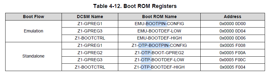
I'm trying to figure out how to configure the bootloader to ignore all GPIO pins and always boot from FLASH.  Looks like according to section 4.3.3.1 in SPRUI33A I need to set Z1-OTP-BOOTPIN-CONFIG = 0x5affffff and BOOTDEF.BOOTDEF0 to 0x03.

How do you write the OTP memory?  The example progranm boot_ex2_customBootConfig appears to only write the emulation boot config registers.  

This project also has this warning in more than one location:

// Change the value of STANDALONE_BOOT to a non-zero value in order to emulate the
// standalone boot process. WARNING: the standalone boot process requires the
// user-configurable DCSM OTP (one-time programmable) registers to be programmed.
// Please ensure the DCSM OTP registers are programmed before choosing to emulate
// the standalone boot process.

This sounds like you must program the OTP registers before you can emulate boot modes.  Is this correct?

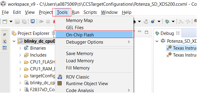
Finally can UniFlash be used for this? 

If so is the menu shown in the attached image the correct location to do so? 

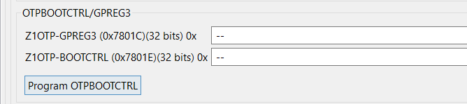
How do the register names used in UniFlash (Z1OTP-BOOTCTRL Z1OTP-GPREG3, Z1OTP-BOOTCTRL Z1OTP-GPREG3) those used in the TRM (Z1-OTP-BOOTPIN-CONFIG, Z1-OTPBOOTDEF-LOW and Z1-OTP-BOOTDEF-HIGH)? I was unable to find addresses in either the datasheet or the TEM.

Do you have to program Z1x and Z2x locations?

Do you need to do anything with the ECC registers?     

Thanks

  • Hi Don, 

    Please take a loot at the training material available at the link provided below and let me know if answers all your questions.  You can specifically study the reset and boot process described in the Reset and Interrupts Module.  See (F28004x Microcontroller Workshop Manual (pdf file) under the heading: Workshop Materials - Revision 1.0 July 2019.  

    training.ti.com/c2000-f28004x-microcontroller-workshop

    Cheers!

    Krishna 

  • Krishna,

    Thank you for the link.  This documentation seems to confirms what I found in 4.3.3.1 of the TRM as far as the values that need to be written to the OTP registers but I was unable to find any information regarding how to program the Z1-OTP-BOOTPIN-CONFIG  and BOOTDEF.BOOTDEF0 registers or their physical addresses.  The figure on page 4-5 gives the starting address but does not specify the address of each register as is typical.  Since these are OTP I would like to be certain.  Can you direct me to specific steps on how to program these memory locations?

    Also the figure on page 4-5 seems to state the EMU registers are used if an emulator is connected and OTP registers otherwise.  This would seem to contradict the assertion I quoted above regarding the need to program the OTP register in order to emulated stand alone operation.  Can you confirm which is correct?

    Thanks

  • Hi,

    On OTP programming, it is programmed using flash API or plug-in (integrated with CCS) like any other flash location. Please note that this can be programmed only once unlike other flash location hence you need to test the feature using emulation boot first. You can also program this field via CCS flash plugin-GUI (CCS -> Tools ) which has specific field for this to program.

    I'll let Krishna answer other query related to "emulating standalone boot".

    Hope this is clear.

    Regards,

    Vivek Singh

  • Vivek,

    I do not have a "tools" menu in the editor perspective.  In the debug perspective there is a tools menu but i do not see a flash GUI entry. (see attached) Where else should I look?

    To use the FLASH API i would need to write a stand alone application to write these two registers?  

    I will need the addresses of the registers in order to use the FLASH API.  I have searched the data sheet for the processor, the TRM, the training module, the boot_ex2_customBootConfog example project and so far have only found the starting location for this memory region, not details of the register location.    Can you tell me where this information is documented?

    Thanks

  • Hi,

    See below the snapshot forom CCS9 -

    Please make sure you launch the target Ist and then only you'll be able to see this.

    After you click on this you'll see following option in GUI to program the OTP field related to BOOTCTRL.

    Regards,

    Vivek Singh

  • The images are not displaying:

  • Don,

    You are on the right track.  All you need to do is to look at the Tool pull down options with  F28004x connected.  You will then be able to open the On-Chip Flash interface.

    Krishna 

  • Sorry, I updated it again.

  • Almost there.  

    Is Z1-OTP-BOOTCTRL the same register as Z1-OTP-BOOTPIN-CONFIG in described the TRM section 4.3.1?

    is Z1-OTP-GPREG3 (32 bits) the same as  Z1-OTPBOOTDEF-LOW and Z1-OTP-BOOTDEF-HIGH (64 bits) in the TRM section 4.3.2?

    Thanks

  • Hi,

    Register mapping is given in "Table 4-12. Boot ROM Registers" of TRM.

    Regards,

    Vivek Singh

  • Those registers in table 4-12 are in ROM and can't be changed.  Looks like what I need is table 4-13, User-Configurable DCSM OTP fields.  Notice that table 4-13 uses underscores in the names instead of dashes as are used in section 4.3.3.1.  That explains why I couldn't find them using search.   

    Thanks

  • Hi Don,

    You also asked about “Emulation Boot Mode”. Please see page 4-6 in the reference link I sent you earlier. To use this mode, configure the target device using the following steps:

    1. Configure EMU-BOOTPIN-CONFIG register
      1. Open a memory window (IDE defaults to 16-bit display mode) at 0xD00
      2. Write at address 0xD00 Value: 0xFFFF
      3. Write at address 0xD01 Value: 0x5AFF
    2. Note that by selecting 0x5A, you are using emulation boot mode without the boot pins and boot mode configured via the OTP
    3. Also note that by selecting 0xFF, 0xFF, 0xFF for BMSP0, BMSP1 and BMSP2 respectively, you are telling the device not to use any GPIO pins in emulation boot mode.
    4. Now configure the Boot Mode by writing to the BOOTDEF registers according to the guidelines on page 4-8 (Boot Mode Definition) in the link I sent you earlier.
      1. In the same memory window opened above at location 0xD00.
      2. Write at address 0xD04 Value: 0x0003 (for Flash) 
      3. Address 0xD05 is a don’t care in this case

    The device is now configured to emulate flash boot. You can load the application to Flash. Apply a reset command from the debugger followed by a run command.  The application will run as it would from flash on power up, except here you have execution (run, step, halt) control via the emulator/IDE.

    Similarly, after you have programmed the OTP, then you can also emulate the OTP boot mode configuration as well. You follow similar steps as explained above, except in step 2 you write an 0xA5FF instead of (0x5AFF).

    Please let us know if you need further assistance.

    Cheers!

    Krishna

  • Krishna,

    My question regarding emulation boot mode was specific to the comments in the demo app stating:

    // Please ensure the DCSM OTP registers are programmed before choosing to emulate
    // the standalone boot process.

    I'm fairly certain this is not correct.  

    Thanks

    Don