This thread has been locked.

If you have a related question, please click the "Ask a related question" button in the top right corner. The newly created question will be automatically linked to this question.

TMS320F28035: DPSWorkshop Lab4 & 5 limit cycle oscillation (LCO) question: Which part of the code in the example project is used to solve LCO problem ??

Part Number: TMS320F28035

I have a question on lab 4 &5 example located at "C:\ti\DPS Workshop_release v2\Workshop\DPS_Workshop".

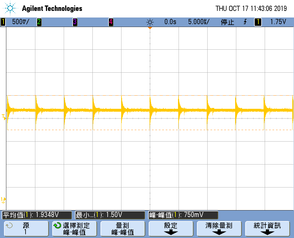
According to DPS Workshop Manual v1.2.pdf, delta Vc needs to design smaller than delta Vs to keep steady state output, no limit cycle.

However, I got confused when I substitute F28335 datasheet parameters into deltaVc&Vs calculation.

delta Vc= Input voltage / DPWM counts under switching frequency(200Khz) = (9V) / (300counts)=30mV 

delta Vs=max ADC input voltage / 12 bits counts = (3.3V) / (2^12) =0.806 mV

Apparently, delta Vc is bigger than delta Vs here which may lead to limit cycle oscillation problem.

I really want to know which part of the code in the example project solve this LCO problem.

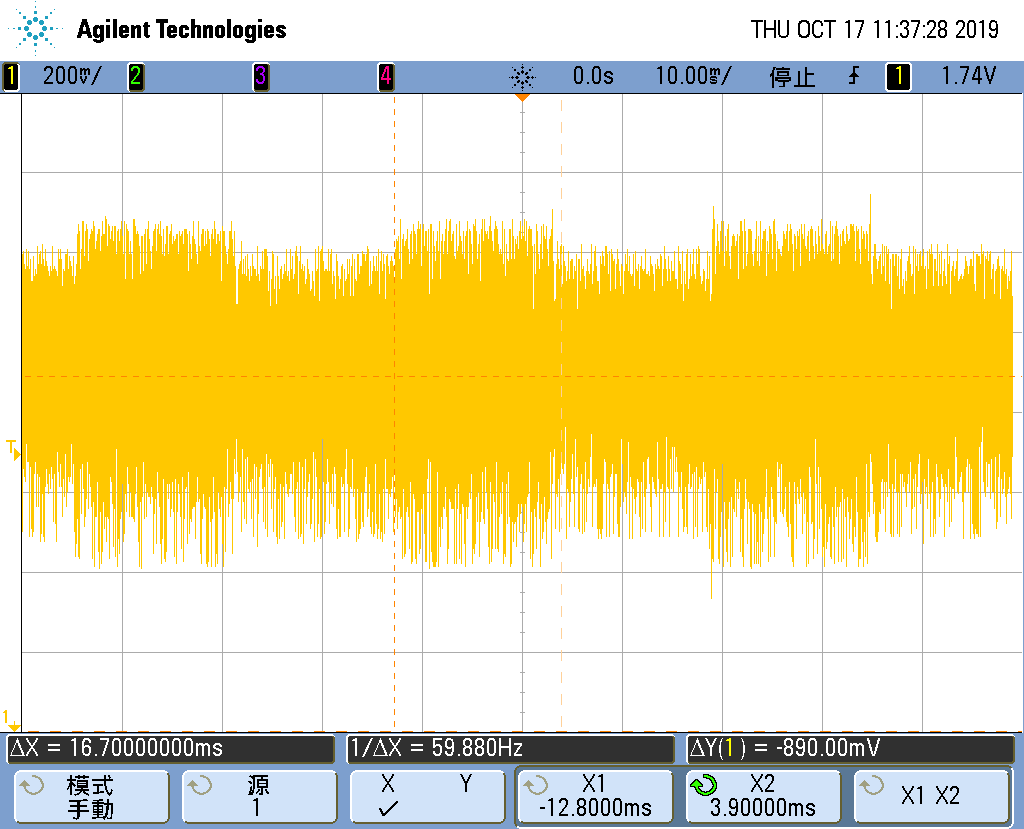
Figure below is the screenshot of the page describing limit cycle in  DPS Workshop Manual v1.2.pdf.


  • There's a little more to it. dVc and dVs have to be relative to the same quantity, for example the output voltage of a VMC buck converter which is what the labs in this workshop, and the plot in your post, are based on.

    Attached is a page which may explain the situation a little more clearly in terms of PWM resolution in bits (N1) and ADC resolution in bits (N2). The condition we are looking for to avoid a limit cycle is

    N1 > N2 - log2(K)

    For a 150MHz device switching at 200kHz I would have expected there to be 750 counts per period, but I guess you are not clocking the PWM module at the full CPU speed(?). Anyway, 300 counts corresponds to a resolution of about 8.23 bits. This is N1.

    N2 is the ADC resolution in bits, i.e. 12.

    K just corresponds to the attenuation in the feedback path to bring the output voltage within the allowable 0-3V range (not 0-3.3V) at the ADC, which is 9V/3V = 1/3, so log2(K) is -1.585.

    We need N1 > 12 + 1.585 = 13.585, but it's only 8.22 so we should expect a limit cycle.

    The feature which can resolve this is HR-PWM, which improves dVc accuracy by increasing the (duty cycle) resolution of the PWM. The principle is outlined in the five workshop slides following the one in your post. With HR mode enabled we have a fixed resolution of about 150ps on the duty edge, so at 200kHz N1 becomes

    N1 = log2(5us/150ps) = log2(33333) = 15.025

    This should be sufficient to prevent the limit cycle. For the F28335, please refer to this document for more information on HR-PWM:
    http://www.ti.com/lit/ug/sprug02b/sprug02b.pdf

    Hope this helps.

    Regards,

    Richard

    limit cycle condition.pdf

  • Thanks for your reply. The attached file helps me a lot.

    I apologize for my mistake that I actually used F28035 not F28335. F28035 is a 60Mhz device with ADC 0V to 3V range.

    K=330 / ( (600//600)+330 )=0.524 based on DPS workshop power stage schematic (Figure.1), so log2(K)= -0.932.

    As mentioned above, N1=8.23 bits, and we need N1 > 12+0.932=12.932, still expects a limit cycle.

    You are right, I am now focus on VMC buck converter.

    I've followed the step and flashed Lab 4 project to F28035 and checked if the code used HR-PWM resource or not(Figure.2).

    http://www.ti.com/lit/ug/sprui10/sprui10.pdf

    Unfortunately, it seems like the project did not use HR mode.

    I measure the Vout-1 on oscilloscope with appropriate control parameters setting provided by the example project but without load transient (Figure.3 &4, Figure.4 is an enlarged view of Figure.3) I am not sure if a limit cycle occurred or not.

    I also measure Vout-1 on oscilloscope under same situation with load transient(Figure.5). An active load is done at a rate of around 30Hz with 50% duty cycle. It seems like the control parameters setting provide low bandwidth?

    According to the results, I suggest that a limit cycle oscillation problem in lab 4 is solved by designing controller to a low bandwidth system ,the concept learned from your attached file(limit cycle condition.pdf), but I am not quite sure about it.

    Please give me some advice. Thank you for all your assistance.


     Figure.1

    Figure.2

    Figure.3

    Figure.4

    Figure.5

  • Thanks for the additional information. Are you using exactly the same board and code as the workshop, or have you made some modifications? If the setup and code is the same you should get a similar Vout-1 graph to that on p.95 of the manual. I've taught this workshop several times and lab 4 normally runs very smoothly.

    From Figure 4 in your last post I don't think we're looking at a limit cycle. I'm going to ask someone with more expertise on power systems to take a look at it.

    I'll get back to you. Thanks for your patience.

    Regards,

    Richard

  • Yes, I am using the same board and code as the workshop without any modifications. I get a similar Vout-1 graph on TI CCS to that on p.95 of the manual but the measurements mentioned above look different from CCS graph.

  • Figure 4 waveform looks like switching noise. Does this corresponds to the switching frequency? I could not clearly read the scale from the plot.

    Shamim

  • Thanks for your reply.

    I am not sure if the waveform result corresponds to the switching noise or not. The DPS workshop power stage's switching noise problem should had been solved  during TI manufacturing process based on my supposition.

    Can you please give me some advice to deal with switching noise problem? I'm afraid that i will accidentally destroy the PCB.

    Besides, can you provide the TI official measuring result of this workshop to me? For example, output voltage and inductor current measurement show on oscilloscope not on CCS.

    Finally, does this workshop tell us that the highest switching frequency of F28035 under same voltage mode controlled structure same as lab4 is 200Khz?  In other words, is it possible to get higher switching frequency with same voltage mode controlled structure? I've read Profiling on C28x targets, but not sure if the calculation time is truely lower than switching period or not.  

  • Based on the plots the switching noise is dominating. It's not a limit cycle. You should be seeing waveforms similar to those on p.96 of the workshop manual.

    It may well be a measurement issue, so it would be worth looking carefully at where and how you are measuring the output voltage.  Ideally, you should be measuring directly across one of the output capacitors (C5 - C7) and have a very short grounding lead. Noise pick-up like this is typical of a long grounding lead in an electrically noisy environment.

    If this doesn't yield any clues, I recommend stepping through lab 4 in the workshop manual, using CCS to graph the output voltage. You should then be seeing cleaner waveforms with the load disturbance active.

    Regards,

    Richard