I am trying to make the example code adc_ppb_delay_cpu01 to work. I am using the control card for TMS320F28379D placed on a custom docking station board.
I am providing voltage inputs to both channels simultaneously which I learnt from this thread. https://e2e.ti.com/support/microcontrollers/c2000/f/171/t/662383
But even then I am seeing different readings from the channels and it seems like that A1 is displaying result by adding up the value of A0 and some offset.
Here are some observations:
Input = 1V to both channels ====> A0 = 380 , A1 = 1390
Input = 2V to both channels ====> A0 = 797, A1 = 2750
Input = 3V to both channels. ====> A0 = 1248, A1 = 4095 (Seems to have maxed out).
Input = 4V to both channels ====> A0 = 1684, A1 = 4095 (maxed again).
Input = 0V to A0 and 1V to A1, ====> A0 = 32, A1 = 1390
Input = 1V to A0 and 0V to A1, ====> A0 = 320, A1 = 0
(All these voltage levels are measured at the controller input pin broken out on the control card just to make sure they are right).
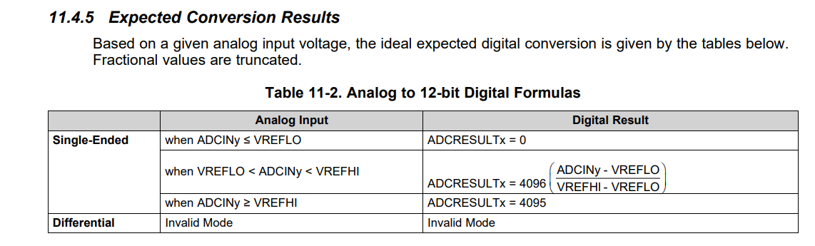
Testing A0 only using a different code, provides the correct values in the A0 register. 4V gives a count of 1290, 2.25V gives a count of 720 and so on. Which can be read easily and made sense of.
Could you please help me in resolving this issue?
I plan to eventually use 4 channels from ADCA itself. So I want independent ADC readings on all 4 channels.