This thread has been locked.

If you have a related question, please click the "Ask a related question" button in the top right corner. The newly created question will be automatically linked to this question.

F28M35H52C: F28M35 Pin configuration issues

Part Number: F28M35H52C


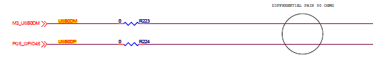
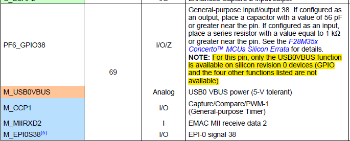
My hardware circuit needs to use external sram, and USB. The pins of these two functions overlap.

As shown below,can I design the connection of the hardware circuit like this? 

  • Hi,

    Are you planning on using EPI Host-bus 8 or 16 signal?

    Looking at table 17-6 and 17-7, it seems HB 8-signal may be suitable with USB usage if you remove the need for the M_USB0PFLT signal, which is an optional signal.

    https://www.ti.com/lit/spruh22

    I wouldn't recommend dual-routing the USB_DP and DM signals as they are meant to be a differential pair. Also USB_VBUS is a 5V signal (dropped to 3.3V before the device pin) I believe.

    Best,

    Kevin

  • user5358342,

    Multiplexing the EPI and USB signals in an application is not recommended.  The two modules are not designed to coexist.  There will be functional contention.

    I recommend prioritizing the USB functionality and reducing the EPI reach.  This can be done by selecting another USB0PFLT option (like GPIO11) instead of GPIO57 and limiting the native EPI memory space to A[12:0] .  Additional memory capacity can be supported through multiple CS spaces, and through paging that is implemented with software-based GPIO control of the higher A[N:13] signals.

    -Tommy

  • 1,I found another problem. The USB_EPEN pin conflicts with the XD3 pin. Whether I use an EPI 8-bit bus or an EPI 16-bit bus.

    As shown below

    2. You said that I don't recommend double routing the USB_DP and DM signals because they are differential pairs. 

    Can I add impedance between these two differential signals to solve the problem?

    3.You said that USB_VBUS is a 5V signal (dropped to 3.3V before the device pin) 

    USB VBUS pin can withstand 5V.

  • In reply to tlee:

    1,I found another problem. The USB_EPEN pin conflicts with the XD3 pin. Whether I use an EPI 8-bit bus or an EPI 16-bit bus.

    As shown below

    2. You said that I don't recommend double routing the USB_DP and DM signals because they are differential pairs. 

    Can I add impedance between these two differential signals to solve the problem?

    3.You said that USB_VBUS is a 5V signal (dropped to 3.3V before the device pin) 

    USB VBUS pin can withstand 5V.

  • Do these two paragraphs explain that the EPIOS41 function and the USB0ID function of the PG6 pin cannot be implemented in the same chip?

  • user5358342 said:
    1,I found another problem. The USB_EPEN pin conflicts with the XD3 pin. Whether I use an EPI 8-bit bus or an EPI 16-bit bus.

    As shown below

    If you search for USB0EPEN in the datasheet, you will find alternate MUX options that do not conflict with EPI.

  • Hi,

    user5358342 said:

    2. You said that I don't recommend double routing the USB_DP and DM signals because they are differential pairs. 

    Can I add impedance between these two differential signals to solve the problem?

    I don't believe so. I'd suggest reading the Application Report on USB signal routing guidelines:

    /cfs-file/__key/communityserver-discussions-components-files/171/USB-2.0-Board-Design-and-Layout-Guidelines.pdf

    user5358342 said:
    USB VBUS pin can withstand 5V.

    Yes, that's right actually. Most of our other devices require VBUS to be dropped down to 3.3V using a resistor, F28M35 being an exception I guess.

    Best,

    Kevin