Other Parts Discussed in Thread: BOOSTXL-DRV8320RS, INA240, EK-TM4C1294XL, , MOTORWARE, TMS320F280049C
Please refer to the TI documented diagrams below refering to external current monitors versus using the internal PGA's.
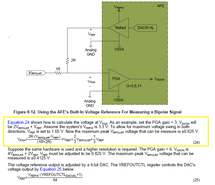
Using the example in 8.6.2.3 page 356-357 Fig.8-12 and Page 230 Fig.5-4 from SPRUHJ1H–January 2013–Revised June 2019:
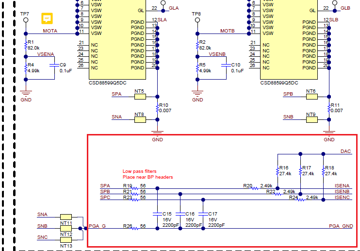
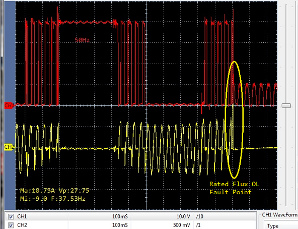
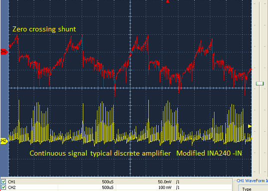
A1: PGA output analog signals seem to zero cross (R19, R22, R25 removed), J5 pins 45, 46, 48 are disconnected.
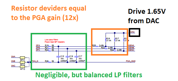
A2: 0R was chosen for R26, R27 PGA_GND since (Rgnd=10k for x3 gain) Fig. 8-12.
1. Please elaborate how does A2 effect PGA output to center 1.65v per formula (yellow box) showing x3 gain?
Formula (yellow box) Fig. 8-12 shows 2*Vbipolar (+/-0.820mv) + Vref (1.65v) = Adcin (3v3).
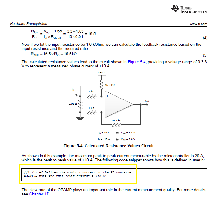
2. Why require PGA set x12 gain for input filter (below) to produce correct results for user ADC scale factor (user.h) ?
3. Will the PGA output (Vadcin) center at (1.65v) as the formula shows for PGA gain set x3?
This point appears important for CMPSS and DAC filter trip behavior.
14.10 Analog Front End Integration
The PGAs operate in concert with the other embedded analog modules (ADC, CMPSS, Buffered DAC) as an analog front end system.
And using external DACA J7 pin 70 for Vref; any time ePWM TripIN zone occurs the DAC Vref level changes to 1.65, was set to 1.35v.
/* Set the DACA output for 1.35v center, INA240 REF1/2 */
DAC_setShadowValue(obj->dacHandle[1], 1646U); //2048
4. Why don't the PGA's seem to ever trip CCMPSS DAC filter fault sample thresholds if they are centered 1.65v per Fig.8-12?
Yet external centered (1.65v) current monitors into analog sub system (TRM: Fig12-4) Gx_ADCAB, GxADCC easily do.
5. Has TI ever tested external current monitors with LauchXLx-49c to verify the DAC filter and scale factor formulas are working as intended?