This thread has been locked.
If you have a related question, please click the "Ask a related question" button in the top right corner. The newly created question will be automatically linked to this question.
In our old board with DSP TMS320C2834 we have a configuration of external memory interface like the figure
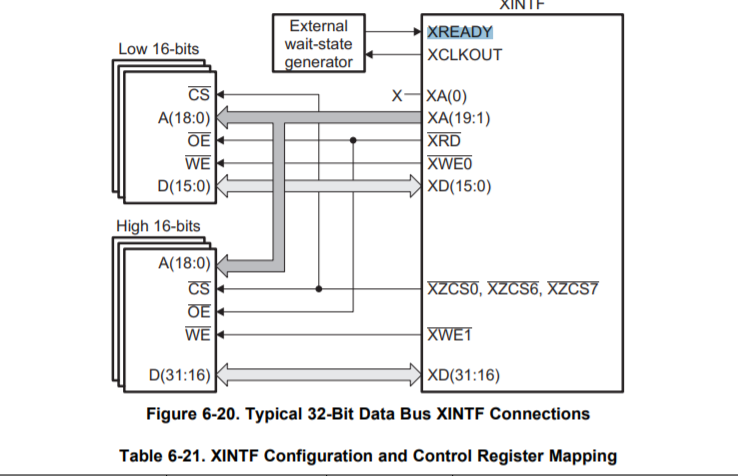
In the second chip we use XWE1 signal connect to WE pin of the RAM.
Is There a signal like this in DSP TMS320F28374D? it is possible to have tow different WE using a 32bit data bus?
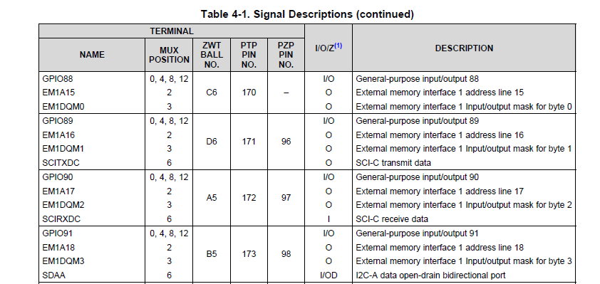
I couldn't use DQM signal because they are busy, I have 18 address, I need the DQM pin used as address bit.
Can I map an other GPIO to DQM function?
ELISA SACCHI said:I couldn't use DQM signal because they are busy, I have 18 address, I need the DQM pin used as address bit.
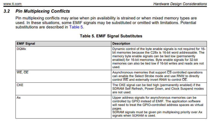
I don't follow how the DQM signals are directly used for 18 addresses. They are byte-mask signals that are optional for 16b memories.
As you could see from the GPIO MUX table take from the TMS320F2837xD Dual-Core Delfino™ Microcontrollers datascheet (http://www.ti.com/lit/ds/symlink/tms320f28379d.pdf Table 4-3. GPIO Muxed Pins ) the pin dedicated to DQM function are multiplexed with address line 15 , 16 17 and 18.
It is possible to configure an other GPIO with DQM function?
Thanks
Elisa,
Thank you for the snapshot. I understand what you mean now.
It is possible to substitute other GPIOs to manually control the DQMn bits, but this can be very inefficient if the program is using mixed 16b- and 32b-accesses. Each access would need to be comprehended and the GPIOs output values updated as necessary. It is similarly possible to substitute other GPIOs to control the higher address bits, but again this can lead to inefficiencies.
Are you using the interface for traditional data storage? If so, you can also consider using SDRAM to replace or extend the SRAM capacity without resorting to GPIOs for manual control. Just know that F2837x cannot execute program instructions out of SDRAM.
This EMIF Appnote has pointers to a reference design and software examples for a mixed SDRAM + SRAM system.
-Tommy
Hi Tommy
Thank for your help, I'm studying whitch could be the better solution for our application. I read the application note you suggest me and I think that the better solution may be using the address most significant bits on GPIO and configure the memory as described in the following table (virtual page).
I can not understand exactly how can define the virtual pages in the FW, there are some example firmware? Application note about that?
Elisa,
Yes there are examples for paging in C2000Ware: ~\C2000Ware_XXXX\device_support\f2837xd\examples\cpu1\emif_dc_pages\cpu01\
Do keep in mind that this approach may require some forethought when designing the software in order to avoid contention between parallel tasks trying to access different pages.
-Tommy
Hi Tommy
Thank you for your help, I need more information about virtual paging.
You can see our linker command file in attach, We map same data and function in external RAM. As we should use the virtual page, how we can define this area on the linker command?
Is it possible to define page with address and gpio configuration?
Inside our code we have function execute in external ram using this pragma directive:
#pragma CODE_SECTION(".ExtRamFuncs");
It will be still possible?
Elisa
/* --COPYRIGHT--,BSD * Copyright (c) $(CPYYEAR), Texas Instruments Incorporated * All rights reserved. * * Redistribution and use in source and binary forms, with or without * modification, are permitted provided that the following conditions * are met: * * * Redistributions of source code must retain the above copyright * notice, this list of conditions and the following disclaimer. * * * Redistributions in binary form must reproduce the above copyright * notice, this list of conditions and the following disclaimer in the * documentation and/or other materials provided with the distribution. * * * Neither the name of Texas Instruments Incorporated nor the names of * its contributors may be used to endorse or promote products derived * from this software without specific prior written permission. * * THIS SOFTWARE IS PROVIDED BY THE COPYRIGHT HOLDERS AND CONTRIBUTORS "AS IS" * AND ANY EXPRESS OR IMPLIED WARRANTIES, INCLUDING, BUT NOT LIMITED TO, * THE IMPLIED WARRANTIES OF MERCHANTABILITY AND FITNESS FOR A PARTICULAR * PURPOSE ARE DISCLAIMED. IN NO EVENT SHALL THE COPYRIGHT OWNER OR * CONTRIBUTORS BE LIABLE FOR ANY DIRECT, INDIRECT, INCIDENTAL, SPECIAL, * EXEMPLARY, OR CONSEQUENTIAL DAMAGES (INCLUDING, BUT NOT LIMITED TO, * PROCUREMENT OF SUBSTITUTE GOODS OR SERVICES; LOSS OF USE, DATA, OR PROFITS; * OR BUSINESS INTERRUPTION) HOWEVER CAUSED AND ON ANY THEORY OF LIABILITY, * WHETHER IN CONTRACT, STRICT LIABILITY, OR TORT (INCLUDING NEGLIGENCE OR * OTHERWISE) ARISING IN ANY WAY OUT OF THE USE OF THIS SOFTWARE, * EVEN IF ADVISED OF THE POSSIBILITY OF SUCH DAMAGE. * --/COPYRIGHT--*/ /* * ======== TMS320C28346.cmd ======== * Define the memory block start/length for the C28346 * *! Revision History *! ================ *! 26-May-2011 jv created to support c28 generic platform. */ /* * PAGE 0 will be used to organize program sections * PAGE 1 will be used to organize data sections * * Notes: * Memory blocks on C28346 are uniform (ie same * physical memory) in both PAGE 0 and PAGE 1. * That is the same memory region should not be * defined for both PAGE 0 and PAGE 1. * Doing so will result in corruption of program * and/or data. */ MEMORY { PAGE 0 : /* Program Memory */ /* BEGIN is used for the "boot to SARAM" bootloader mode */ BEGIN : origin = 0x000000, length = 0x000002 /* Boot to M0 will go here */ H05SARAM : origin = 0x300000, length = 0x030000 /* on-chip RAM block H0-H5 */ CSM_RSVD : origin = 0x33FF80, length = 0x000076 /* Reserved - for compatibility to legacy C28x designs. */ CSM_PWL : origin = 0x33FFF8, length = 0x000008 /* 128-bit password locations */ IQTABLES : origin = 0x3FE000, length = 0x000b50 IQTABLES2 : origin = 0x3FEB50, length = 0x00008c FPUTABLES : origin = 0x3FEBDC, length = 0x0006A0 BOOTROM : origin = 0x3FF27C, length = 0x000D44 RESET : origin = 0x3FFFC0, length = 0x000002 EXT7P0 : origin = 0x200000, length = 0x030000 //L0SARAM : origin = 0x008000, length = 0x002000 /* on-chip RAM block L0 for fastfunc not used anymore no only 1% faster*/ PAGE 1 : M01SARAM : origin = 0x000002, length = 0x0007FE /* on-chip RAM block M0, M1 */ PIEVECT : origin = 0xD00, length = 0x100 L03SARAM : origin = 0x008000, length = 0x08000 /* on-chip RAM block L0-L3, also used by bootloader, do not put initilized data here, can be used for stack*/ L47SARAM : origin = 0x010000, length = 0x08000 /* on-chip RAM block L4-L7, also used by bootloader, do not put initilized data here*/ EXT7SARAM : origin = 0x230000, length = 0x0D0000 /* external SRAM 65535 *16 bits*/ SDRAMP1 : origin = 0x180000, length = 0x080000 /* external SDRAM on FPGA*/ } /* * Allocate sections to memory blocks. * Note: * codestart user defined section in DSP28_CodeStartBranch.asm * used to redirect code execution when booting to flash */ /* Table 4-1. Initialized Sections Created by the Compiler Name Contents Restrictions .cinit Tables for explicitly initialized global and static variables Program .const Global and static const variables that are explicitly Low 64K initialized and contain string literals .econst Far constant variables Anywhere in data .pinit Table of constructors to be called at startup Program .switch Jump tables for large switch statements Program with -mt option Data without -mt option .text Executable code and constants Program Table 4-2. Uninitialized Sections Created by the Compiler Name Contents Restrictions .bss Global and static variables Low 64K .ebss Far global/static variables Anywhere in data .stack Stack Low 64K .sysmem Memory for malloc functions (heap) Low 64K .esysmem Memory for far_malloc functions Anywhere in data */ SECTIONS { /* Allocate program areas: */ // myUFFS : { uffs* (*)} > EXT7SARAM PAGE = 1 //myXML : { rapidxml*.obj (*) TestFile*.obj (*) Xml*.obj (*)} > EXT7SARAM PAGE = 1 .FbDpRamBuffers : > EXT7SARAM PAGE = 1 CamBuffer : > EXT7SARAM PAGE = 1 .SlowSdRam : > SDRAMP1 PAGE = 1 TraceBuffer : > SDRAMP1 PAGE = 1 /* Used before external RAM is initialised. */ .EarlyFuncs : { halXIntfDsp28x.obj(.text) } > H05SARAM PAGE = 0 .ExtRamFuncs : { /*Put this functions to slower external RAM*/ ServoDriveInit.obj(.text .econst) Xml*.obj(.text .econst) uffs_*.obj(.text .econst) CamXmlImport.obj(.text .econst) CCamActionFactory.obj(.text .econst) CCamExitIdFactory.obj(.text .econst) ErrorHistory.obj(.text .econst) UsageState.obj(.text .econst) *CamBuilder.obj(.text .econst) *CamFactory*.obj(.text .econst) CamComponentBuilder.obj(.text .econst) aes.obj(.text .econst) ConfigParam*.obj(.text .econst) AesFileEncryption.obj(.text .econst) /* All .init() methods. */ *.obj(.text:_init__*) } > EXT7P0 PAGE = 0 .SlowSdFuncs > EXT7P0 PAGE = 0 .cinit : > EXT7P0 PAGE = 0 .pinit : > H05SARAM PAGE = 0 .text : > H05SARAM PAGE = 0 ramfuncs : > H05SARAM PAGE = 0 codestart : > H05SARAM PAGE = 0 csmpasswds : > CSM_PWL PAGE = 0 csm_rsvd : > CSM_RSVD PAGE = 0 /* Initalized sections */ //.econst : > H05SARAM PAGE = 0 .econst : > EXT7P0 PAGE = 0 .switch : > H05SARAM PAGE = 0 // .args : > H05SARAM PAGE = 0 .ExtRam : { /*Put this functions to slower external RAM*/ Xml*.obj(.ebss) uffs_*.obj(.ebss) uffsConfigSpi.obj (.ebss) CamXmlImport.obj(.ebss) ErrorHistory.obj(.ebss) *CamBuilder.obj(.ebss) *CamFactory*.obj(.ebss) aes.obj(.ebss) AmaMode.obj(.ebss) ConfigParam*.obj(.ebss) AesFileEncryption.obj(.ebss) //app_p28FP.o28FP (.ebss) } > EXT7SARAM PAGE = 1 BIOS_DEBUG_LOGGER : > EXT7SARAM PAGE = 1 BIOS_DEBUG : > EXT7SARAM PAGE = 1 /* * Allocate data sections: */ /* Assign fast internal RAM to the stacks. */ .taskStack : > L03SARAM PAGE = 1 .stack : > M01SARAM PAGE = 1 /* General globals/statics gets the leftovers. */ .ebss : >> L03SARAM | M01SARAM | L47SARAM PAGE = 1 /* Heap (far_malloc). */ .esysmem : > L47SARAM PAGE = 1 /* C I/O buffers, e.g. for printf(), small but not used after init. */ .cio : > EXT7SARAM PAGE = 1 /* Specific globals/statics. */ .sysHeap : > L47SARAM PAGE = 1 .PatternBuffers : > L47SARAM PAGE = 1 .ObjDict : > L47SARAM PAGE = 1 /* Global/static too big for internal memory. */ .UFFSTab : > EXT7SARAM PAGE = 1 /* Allocate IQ math areas: */ IQmath : > H05SARAM PAGE = 0 IQmathTables : > IQTABLES PAGE = 0, TYPE = NOLOAD /* * Uncomment the section below if calling the IQNexp() or IQexp() * functions from the IQMath.lib library in order to utilize the * relevant IQ Math table in Boot ROM (This saves space and Boot ROM * is 1 wait-state). If this section is not uncommented, IQmathTables2 * will be loaded into other memory (SARAM, Flash, etc.) and will take * up space, but 0 wait-state is possible. */ /* IQmathTables2 : > IQTABLES2 PAGE = 0, TYPE = NOLOAD { IQmath.lib<IQNexpTable.obj> (IQmathTablesRam) } */ FPUmathTables : > FPUTABLES PAGE = 0, TYPE = NOLOAD }
Elisa,
I would not recommend using GPIO paging when executing out of EMIF. It will be too problematic.
Can you describe the target external memory system? How many ICs? Word size? Capacity?
-Tommy
I Tommy
We analyzed all possibility about our system, in actual board we have code and data located on the external memory and we can access the Memory even at 16 and 32 bit data bus using WE0 and WE1.
As you tell me, there are no way to do the same using the new DSP.
If we map the code in the first page, it is possible to use DMA and paging for data access (in the others page)?
ELISA SACCHI said:We analyzed all possibility about our system, in actual board we have code and data located on the external memory and we can access the Memory even at 16 and 32 bit data bus using WE0 and WE1.As you tell me, there are no way to do the same using the new DSP.
This capability is supported, but as you have pointed out, not without the sacrifice of some higher address signals because of pinmuxing. How much external memory do you require in the application for program and data?
ELISA SACCHI said:If we map the code in the first page, it is possible to use DMA and paging for data access (in the others page)?
This will only be practical if you can guarantee that the CPU will not execute out of external memory while data is being accessed in paged memory.
The newer F2838x series of devices could be another option. My understanding is that the first 1Mx16 of CS0 SDRAM memory can be dual-mapped to executable memory space so that SDRAM can be used for both program and data.
Elisa,
Another thought is that if you do not need all of the EMIF address signals, you can allocate two to DQMn functions with the trade-off of making the memory range non-contiguous from the C28x perspective.
For example, if you only need 18 out of the 20 address signals (so typically A0-A17), you can configure the pinmux as such:
GPIO # | EMIF SIGNAL | MEMORY SIGNAL |
Multiple | EM1A0 .. EM1A15 | ADDR0 .. ADDR15 |
89 | EM1DQM1 | WE0 |
90 | EM1DQM2 | WE1 |
91 | EM1A18 | ADDR16 |
92 | EM1A19 | ADDR17 |
This would give the C28x a logical view of 4-pages x 64-Kwords x 32-bits that are controlled by the EMIF with no need for manual GPIO control. The pages could also be abstracted from the program by combining the multiple pages into a single memory section in the CMD file.
-Tommy
Hi Tommy
Thank you very much for your patience, this solution could certainly be the best for our proposal!!
Elisa
Elisa,
I'm glad that this is looking more acceptable for your system. I feel obligated to point out that I have not verified this proposal on bench and will not have access to any hardware to do so in the near future. I sincerely believe that this will work, but I don't have experimental proof.
-Tommy