- Ask a related questionWhat is a related question?A related question is a question created from another question. When the related question is created, it will be automatically linked to the original question.

Tool/software: Code Composer Studio
Hi,my project is work on CCS10, I import the example project "spi_ex2_dma_loopback",my F280049 board can run this project correctly.
I want make some datas from SPIB to SPIA by using DMA base on this example project ,so i shut down loopback mode, add GPIOs configuration and changed some place,but DMA can not move datas from SPIRXBUF to RAM,my code below here:
#define BURST (FIFO_LVL - 1) // burst size should be less than 8
#define TRANSFER 15 // [(MEM_BUFFER_SIZE/FIFO_LVL)-1]
#define FIFO_LVL 8 // FIFO Interrupt Level
#pragma DATA_SECTION(sdata, "ramgs0"); // map the TX data to memory
#pragma DATA_SECTION(rdata, "ramgs1"); // map the RX data to memory
uint16_t sdata[128]; // Send data buffer
uint16_t rdata[128]; // Receive data buffer
DMAInitialize();
DMASource = (volatile uint16_t *)sdata;
DMADest = (volatile uint16_t *)rdata;
//
// configure DMACH5 for TX
//
DMACH5AddrConfig(&SpibRegs.SPITXBUF,DMASource);
DMACH5BurstConfig(BURST,1,0); // Burst size, src step, dest step
DMACH5TransferConfig(TRANSFER,1,0); // transfer size, src step, dest step
DMACH5ModeConfig(DMA_SPIBTX,PERINT_ENABLE,ONESHOT_DISABLE,CONT_DISABLE,SYNC_DISABLE,SYNC_SRC,OVRFLOW_DISABLE,SIXTEEN_BIT,CHINT_END,CHINT_ENABLE);
//
// configure DMA CH2 for RX
//
DMACH6AddrConfig(DMADest,&SpiaRegs.SPIRXBUF);
DMACH6BurstConfig(BURST,0,1);
DMACH6TransferConfig(TRANSFER,0,1);
DMACH6ModeConfig(DMA_SPIARX,PERINT_ENABLE,ONESHOT_DISABLE,CONT_DISABLE,SYNC_DISABLE,SYNC_SRC,OVRFLOW_DISABLE,SIXTEEN_BIT,CHINT_END,CHINT_ENABLE);
SpiaRegs.SPIFFRX.all=0x2040; // RX FIFO enabled, clear FIFO int
SpiaRegs.SPIFFRX.bit.RXFFIL = FIFO_LVL; // Set RX FIFO level
SpibRegs.SPIFFTX.all=0xE040; // FIFOs enabled, TX FIFO released,
SpibRegs.SPIFFTX.bit.TXFFIL = FIFO_LVL; // Set TX FIFO level
GpioCtrlRegs.GPAPUD.bit.GPIO8 = 0;
GpioCtrlRegs.GPAPUD.bit.GPIO9 = 0;
GpioCtrlRegs.GPAPUD.bit.GPIO10 = 0;
GpioCtrlRegs.GPAPUD.bit.GPIO11 = 0;
GpioCtrlRegs.GPAQSEL1.bit.GPIO8 = 3;
GpioCtrlRegs.GPAQSEL1.bit.GPIO9 = 3;
GpioCtrlRegs.GPAQSEL1.bit.GPIO10 = 3;
GpioCtrlRegs.GPAQSEL1.bit.GPIO11 = 3;
GpioCtrlRegs.GPAGMUX1.bit.GPIO8 = 1; // SPISIMOA
GpioCtrlRegs.GPAGMUX1.bit.GPIO9 = 1; // SPICLKA
GpioCtrlRegs.GPAGMUX1.bit.GPIO10 = 1; // SPISOMIA
GpioCtrlRegs.GPAGMUX1.bit.GPIO11 = 1; // SPISTEA
GpioCtrlRegs.GPAMUX1.bit.GPIO8 = 3; // SPISIMOA
GpioCtrlRegs.GPAMUX1.bit.GPIO9 = 3; // SPICLKA
GpioCtrlRegs.GPAMUX1.bit.GPIO10 = 3; // SPISOMIA
GpioCtrlRegs.GPAMUX1.bit.GPIO11 = 3; // SPISTEA
GpioCtrlRegs.GPAPUD.bit.GPIO24 = 0;
GpioCtrlRegs.GPAPUD.bit.GPIO25 = 0;
GpioCtrlRegs.GPAPUD.bit.GPIO26 = 0;
GpioCtrlRegs.GPAPUD.bit.GPIO27 = 0;
GpioCtrlRegs.GPAQSEL2.bit.GPIO24 = 3;
GpioCtrlRegs.GPAQSEL2.bit.GPIO25 = 3;
GpioCtrlRegs.GPAQSEL2.bit.GPIO26 = 3;
GpioCtrlRegs.GPAQSEL2.bit.GPIO27 = 3;
GpioCtrlRegs.GPAGMUX2.bit.GPIO24 = 1; // SPISIMOB
GpioCtrlRegs.GPAGMUX2.bit.GPIO25 = 1; // SPIS0MIB
GpioCtrlRegs.GPAGMUX2.bit.GPIO26 = 1; // SPICLKB
GpioCtrlRegs.GPAGMUX2.bit.GPIO27 = 1; // SPISTEB
GpioCtrlRegs.GPAMUX2.bit.GPIO24 = 2; // SPISIMOB
GpioCtrlRegs.GPAMUX2.bit.GPIO25 = 2; // SPIS0MIB
GpioCtrlRegs.GPAMUX2.bit.GPIO26 = 2; // SPICLKB
GpioCtrlRegs.GPAMUX2.bit.GPIO27 = 2; // SPISTEB
SpibRegs.SPICCR.bit.SPISWRESET = 0;
SpibRegs.SPICCR.bit.CLKPOLARITY = 0;
SpibRegs.SPICCR.bit.SPICHAR = (16-1);
SpibRegs.SPICTL.bit.MASTER_SLAVE = 1;
SpibRegs.SPICTL.bit.TALK = 1;
SpibRegs.SPICTL.bit.CLK_PHASE = 0;
SpibRegs.SPICTL.bit.SPIINTENA = 0;
SpibRegs.SPIBRR.bit.SPI_BIT_RATE = SPI_BRR;
SpibRegs.SPIPRI.bit.FREE = 1;
SpibRegs.SPICCR.bit.SPISWRESET = 1;
SpiaRegs.SPICCR.bit.SPISWRESET = 0;
SpiaRegs.SPICCR.bit.CLKPOLARITY = 0;
SpiaRegs.SPICCR.bit.SPICHAR = (16-1);
SpiaRegs.SPICTL.bit.MASTER_SLAVE = 0;
SpiaRegs.SPICTL.bit.TALK = 1;
SpiaRegs.SPICTL.bit.CLK_PHASE = 0;
SpiaRegs.SPICTL.bit.SPIINTENA = 0;
SpiaRegs.SPIPRI.bit.FREE = 1;
SpiaRegs.SPICCR.bit.SPISWRESET = 1;
for(i=0; i<128; i++)
{
sdata[i] = i;
rdata[i]= 0;
}
PieCtrlRegs.PIECTRL.bit.ENPIE = 1; // Enable the PIE block
PieCtrlRegs.PIEIER7.bit.INTx5 = 1; // Enable PIE Group 7, INT 1 (DMA CH1)
PieCtrlRegs.PIEIER7.bit.INTx6 = 1; // Enable PIE Group 7, INT 2 (DMA CH2)
IER= M_INT7; // Enable CPU INT6
EINT; // Enable Global Interrupts
StartDMACH6(); // Start SPI RX DMA channel
StartDMACH5(); // Start SPI TX DMA channel
I connected GPIO8 TO GPIO24 , GPIO9 TO GPIO26 , GPIO10 TO GPIO25 , GPIO11 TO GPIO27,then run this new project,
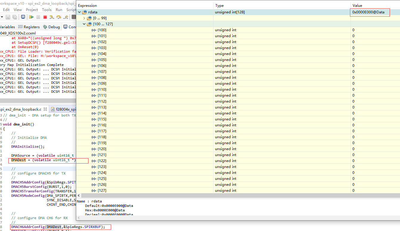
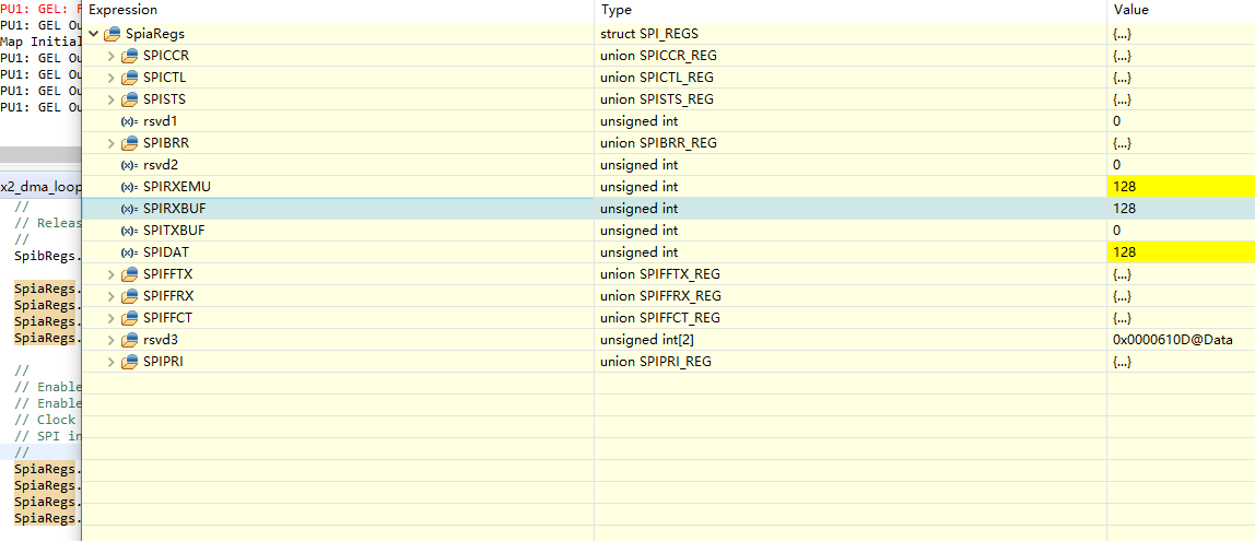
I found the DMA can move sdata[] to SPIBTXBUF,and SPIARXBUF had correct data,but DMA can not move data from SPIARXBUF to rdata[].
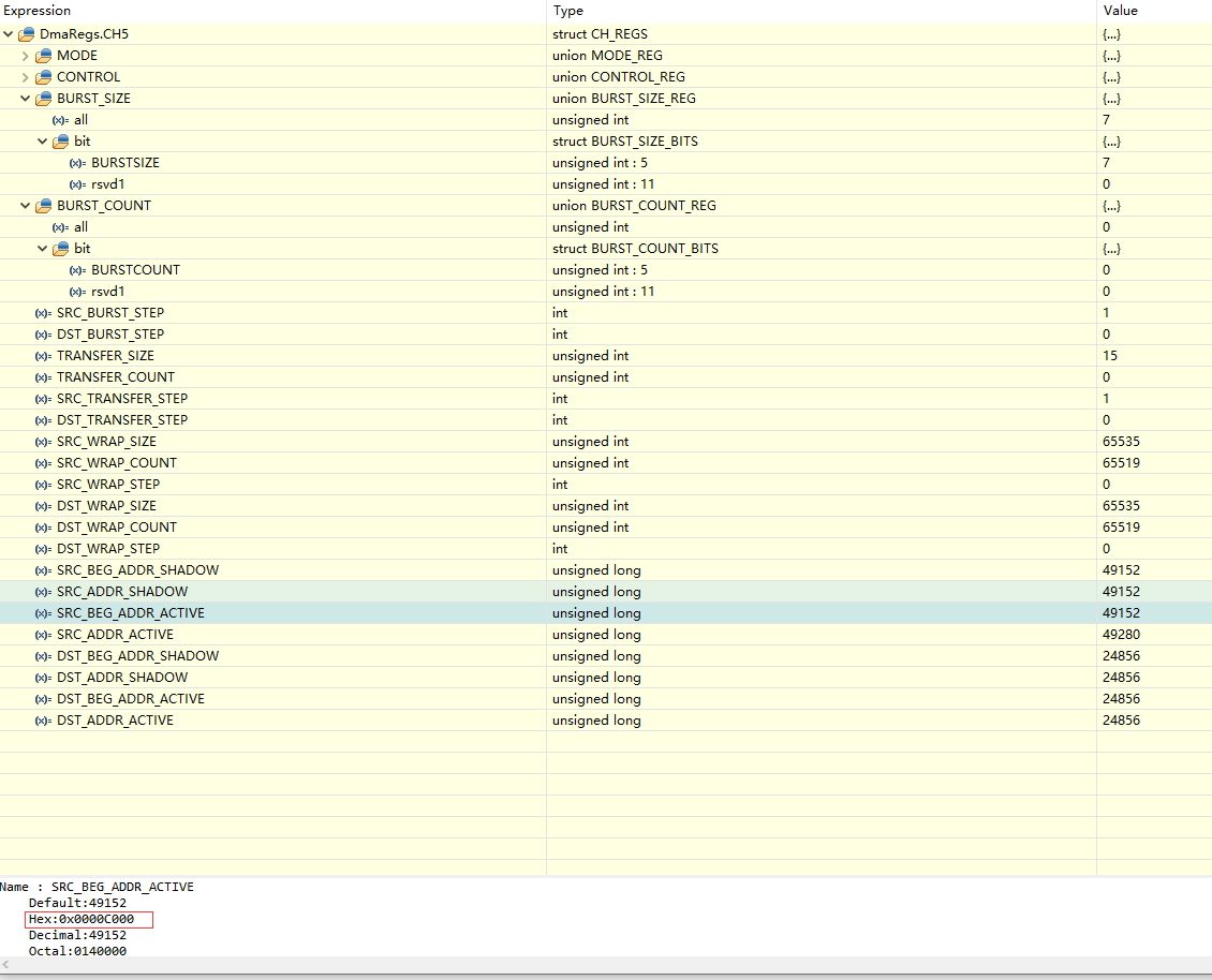
Suspend and DEBUG , I found the RUNSTS bit of CH6 CONTROL is 1.

So DMA CH6 is run ,but can nor work?
Please help me to solve the problem,thanks!