


Part Number: TMS320F280049
Other Parts Discussed in Thread: ADS1248
Hi team,
I am using the following code for interfacing ADC ADS1248 with tms320f280049 micro controller. While going through datasheet of ADS1248 I found that the clock polarity and clock phase should be 0 and 1 respectively. The figure below is the snippet from pseudo code provided in ADS1248 datasheet.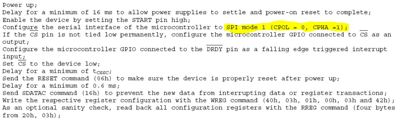
But when I used the said configuration I didn`t got the output as expected when I made a register read back operation with RREG command. When I used clock polarity and clock phase value both zero I got the result as expected. Is there is any reason for having this sort of problem or am I getting the correct read back value accidentally. Will it affect my future readings ? Is there is any way that I can get single conversions done by ADC while I am using it, otherwise to keep it off or in non operative mode without affecting already set values of configuration registers.
void main(void)
{
// Intiate system controls, GPIO pins
uint16_t r1 = 0x0000;
uint16_t r2 = 0x0000;
InitSysCtrl();
InitGpio();
EALLOW;
GpioCtrlRegs.GPAGMUX1.bit.GPIO9 = 1;
GpioCtrlRegs.GPAMUX1.bit.GPIO9 = 3; // set Gpio pin 9 as SPI clock pin
GpioCtrlRegs.GPAPUD.bit.GPIO9 = 0; // Pull up enable
GpioCtrlRegs.GPAQSEL1.bit.GPIO9 = 3; // Qualifier Selection
GpioCtrlRegs.GPAGMUX1.bit.GPIO8 = 1;
GpioCtrlRegs.GPAMUX1.bit.GPIO8 = 3; // set Gpio pin 8 as SPI SIMO pin
GpioCtrlRegs.GPAPUD.bit.GPIO8 = 0; // Pull up enable
GpioCtrlRegs.GPAQSEL1.bit.GPIO8 = 3; // Qualifier Selection
GpioCtrlRegs.GPAGMUX1.bit.GPIO10 = 1;
GpioCtrlRegs.GPAMUX1.bit.GPIO10 = 3; // set Gpio pin 10 as SPI SOMI pin
GpioCtrlRegs.GPAPUD.bit.GPIO10 = 0; // Pull up enable
GpioCtrlRegs.GPAQSEL1.bit.GPIO10 = 3; // Qualifier Selection
GpioCtrlRegs.GPAGMUX1.bit.GPIO14 = 0;
GpioCtrlRegs.GPAMUX1.bit.GPIO14 = 0; // set Gpio pin 14 as GPIO output pin (CS/)
GpioCtrlRegs.GPADIR.bit.GPIO14 = 1; // set direction as output
GpioCtrlRegs.GPAGMUX1.bit.GPIO15 = 0;
GpioCtrlRegs.GPAMUX1.bit.GPIO15 = 0; // set Gpio pin 15 as GPIO output pin (START)
GpioCtrlRegs.GPADIR.bit.GPIO15 = 1; // set direction as output
GpioCtrlRegs.GPBGMUX1.bit.GPIO34 = 0;
GpioCtrlRegs.GPBMUX1.bit.GPIO34 = 0; // set Gpio pin 34 as GPIO output pin (ADC_RST)
GpioCtrlRegs.GPBDIR.bit.GPIO34 = 1; // set direction as output (ADC_RST)
GpioCtrlRegs.GPAGMUX1.bit.GPIO6 = 0;
GpioCtrlRegs.GPAMUX1.bit.GPIO6 = 0; // set Gpio pin 6 as GPIO input pin (IRQ_3)
InputXbarRegs.INPUT4SELECT = 0x6; // GPIO6 is selected as interrupt 1 input
EDIS;
GpioDataRegs.GPASET.bit.GPIO14 = 1; // Clear CS/ pin to high
GpioDataRegs.GPACLEAR.bit.GPIO15 = 1; // ADC_RST held low
GpioDataRegs.GPBCLEAR.bit.GPIO34 = 1; // START pin held low
SpiaRegs.SPICCR.bit.SPISWRESET = 0; // clear software reset bit
SpiaRegs.SPICTL.bit.MASTER_SLAVE = 1; // master mode selected
SpiaRegs.SPICTL.bit.CLK_PHASE = 0; // clock phase selection
SpiaRegs.SPICCR.bit.CLKPOLARITY = 0; // clock polarity
SpiaRegs.SPIBRR.bit.SPI_BIT_RATE = 24; //(25MHz/25 = 1 MHz)
SpiaRegs.SPICCR.bit.SPICHAR = 15; // character per transfer
SpiaRegs.SPISTS.bit.INT_FLAG = 0; // clear interrupt flag
SpiaRegs.SPISTS.bit.OVERRUN_FLAG = 0; // clear over run flag
SpiaRegs.SPIPRI.bit.FREE = 1;
SpiaRegs.SPICCR.bit.SPILBK = 0; // loop back enable
SpiaRegs.SPICTL.bit.TALK = 1; // slave talk enabled
SpiaRegs.SPICTL.bit.SPIINTENA = 0; // interrupt enable
SpiaRegs.SPICCR.bit.SPISWRESET = 1; // software reset disabled
GpioDataRegs.GPACLEAR.bit.GPIO14 = 1; // Clear CS/ pin to low
GpioDataRegs.GPBSET.bit.GPIO34 = 1; // ADC_RST disabled
GpioDataRegs.GPASET.bit.GPIO15 = 1; // Enable the device by setting START pin high
SpiaRegs.SPITXBUF = 0xFF06; // Send the RESET command and wait for 0.6ms
DELAY_US(600);
SpiaRegs.SPITXBUF = 0x1640; // Send the SDATAC command and WREG Command 1st byte
SpiaRegs.SPITXBUF = 0x030A; // WREG Command 2nd byte and MUX0 register value
SpiaRegs.SPITXBUF = 0x0020; // VBIAS register value and MUX1 register value
SpiaRegs.SPITXBUF = 0x404A; // SYS0 register and WREG 1st command byte
SpiaRegs.SPITXBUF = 0x0105; // WREG 2nd command byte and IDAC0 register value
SpiaRegs.SPITXBUF = 0x03FF; // IDAC1 register value and ADC sync command
SpiaRegs.SPITXBUF = 0x2003; // RREG 1st and RREG 2nd byte
SpiaRegs.SPITXBUF = 0xFFFF; // RREG 1st and RREG 2nd byte
SpiaRegs.SPITXBUF = 0xFF02; // NOP command
DELAY_US(500);
SpiaRegs.SPITXBUF = 0x0004; // NOP command and SYNC command to start a new conversion
while(GpioDataRegs.GPADAT.bit.GPIO6 != 0) // checking DRDY for low value on it
{
}
DELAY_US(1);
SpiaRegs.SPITXBUF = 0xFF12; // NOP and RDATA
SpiaRegs.SPITXBUF = 0xFFFF; // NOP commands
r1 = SpiaRegs.SPIRXBUF; // first 16 bits of conversion result MSB first
SpiaRegs.SPITXBUF = 0xFF02; // NOP and SLEEP command
r2 = SpiaRegs.SPIRXBUF; // Second 8 bits of conversion result and remaining 8 bits of junk value
for(;;)
{
}
}
Regards,
Vineeth

