Part Number: TMS320F28335
Dear team:
I have a customer who uses the XINTF interface to communicate with FPGA, but cannot write data. The following is a detailed description:
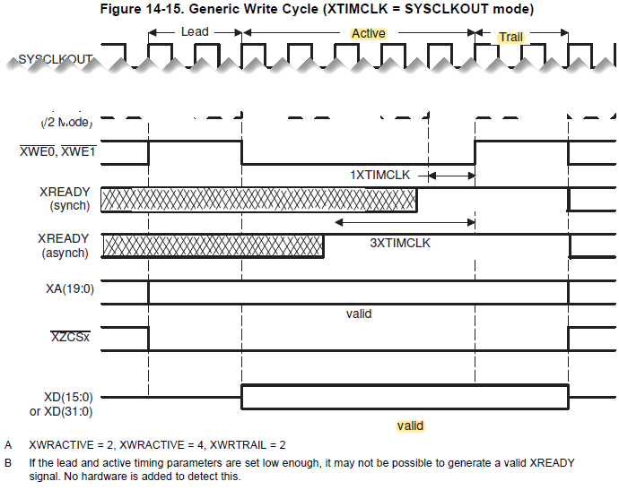
XINTF configuration is as follows:
void InitXintf(void) {
// This shows how to write to the XINTF registers. The
// values used here are the default state after reset.
// Different hardware will require a different configuration.

// For an example of an XINTF configuration used with the
// F28335 eZdsp, refer to the examples/run_from_xintf project.

// Any changes to XINTF timing should only be made by code
// running outside of the XINTF.

// All Zones---------------------------------
// Timing for all zones based on XTIMCLK = 1/2 SYSCLKOUT
EALLOW;
SysCtrlRegs.PCLKCR3.bit.XINTFENCLK = 1;
EDIS;


EALLOW;
XintfRegs.XINTCNF2.bit.XTIMCLK = 1;
// No write buffering
XintfRegs.XINTCNF2.bit.WRBUFF = 0;
// XCLKOUT is enabled
XintfRegs.XINTCNF2.bit.CLKOFF = 0;
// XCLKOUT = XTIMCLK/2
XintfRegs.XINTCNF2.bit.CLKMODE = 1;

// Zone 0------------------------------------
// When using ready, ACTIVE must be 1 or greater
// Lead must always be 1 or greater
// Zone write timing
XintfRegs.XTIMING0.bit.XWRLEAD = 3;
XintfRegs.XTIMING0.bit.XWRACTIVE = 7;
XintfRegs.XTIMING0.bit.XWRTRAIL = 3;
// Zone read timing
XintfRegs.XTIMING0.bit.XRDLEAD = 3;
XintfRegs.XTIMING0.bit.XRDACTIVE = 7;
XintfRegs.XTIMING0.bit.XRDTRAIL = 3;

// double all Zone read/write lead/active/trail timing
XintfRegs.XTIMING0.bit.X2TIMING = 1;

// Zone will sample XREADY signal
XintfRegs.XTIMING0.bit.USEREADY = 1; //修改值,忽略xready信号
XintfRegs.XTIMING0.bit.READYMODE = 1; // sample asynchronous

// Size must be either:
// 0,1 = x32 or
// 1,1 = x16 other values are reserved
XintfRegs.XTIMING0.bit.XSIZE = 3;
EDIS;

}
Use ZONE0 area, the communication code is as follows:
void CommunicationFPGA(void)
{


                GpioDataRegs.GPACLEAR.bit.GPIO5 = 1;            //D_G_A 使能A相数据总线收发器
                GpioDataRegs.GPASET.bit.GPIO30 = 1;             //D_G_B 禁止B相总线收发器导通
                GpioDataRegs.GPBSET.bit.GPIO32 = 1;             //D_G_C 禁止C相总线收发器导通

                GpioDataRegs.GPACLEAR.bit.GPIO2 = 1;           //A_G_A****地址线总线收发器使能,低电平使能
                GpioDataRegs.GPASET.bit.GPIO1 = 1;             //A_G_B地址总线禁止
                GpioDataRegs.GPBSET.bit.GPIO39 = 1;            //A_G_C

                GpioDataRegs.GPASET.bit.GPIO4 = 1;             //D_DIR_A 总线收发器方向,DSP->FPGA
                GpioDataRegs.GPASET.bit.GPIO3 = 1;

                *(sendStart + 0) =Value;               //Value = 9.
                *(sendStart + 1) =Value;
                *(sendStart + 2) =Value;
                *(sendStart + 3) =Value;
                *(sendStart + 4) =Value;
                *(sendStart + 5) =Value;
                *(sendStart + 6) =Value;
                *(sendStart + 7) =Value;


                GpioDataRegs.GPACLEAR.bit.GPIO4 = 1;             //D_DIR_A 总线收发器方向,FPAG->DSP
                GpioDataRegs.GPASET.bit.GPIO3 = 1;
            /*  receFPGAmessage[0] = *(receStart + 0);    //第一个子模块电压
                receFPGAmessage[1] = *(receStart + 1);    //第二个子模块电压
                receFPGAmessage[2] = *(receStart + 2);    //第三个子模块电压
                receFPGAmessage[3] = *(receStart + 3);    //第三个子模块电压
                receFPGAmessage[4] = *(receStart + 4);    //第四个子模块电压
                receFPGAmessage[5] = *(receStart + 5);
                receFPGAmessage[6] = *(receStart + 6);
                receFPGAmessage[7] = *(receStart + 7);    //第六个子模块电压

                receFPGAmessage[8] = *(receStart + 8);    //第七个子模块电压
                receFPGAmessage[9] = *(receStart + 9);    //第七个子模块电压
                receFPGAmessage[10] = *(receStart + 10);    //第八个子模块电压
                receFPGAmessage[11] = *(receStart + 11);    //第八个子模块电压
                receFPGAmessage[12] = *(receStart + 12);    //第八个子模块电压
                receFPGAmessage[13] = *(receStart + 13);    //第八个子模块电压
                receFPGAmessage[14] = *(receStart + 14);    //第八个子模块电压
                receFPGAmessage[15] = *(receStart + 15);    //第八个子模块电压*/

                GpioDataRegs.GPASET.bit.GPIO5 = 1;              //D_G_A 禁止A相数据总线收发器
                GpioDataRegs.GPASET.bit.GPIO2 = 1;             //A_G_A禁止A相地址总线收发

                return;
}
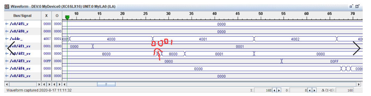
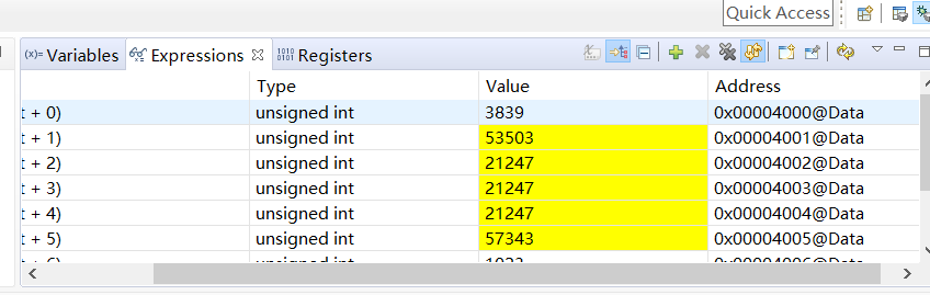
During the simulation, by viewing the Expressions window, it was found that the data was abnormal and there was no pattern.
I have tested that the FPGA timing is correct.
What could cause the problem?
Best regards