
- Ask a related questionWhat is a related question?A related question is a question created from another question. When the related question is created, it will be automatically linked to the original question.
Original question:

Tool/software: Code Composer Studio
Hi all, I got a very weird issue on 28335 xintf interface right now. In my board, I connected low data bus(bit15~0) xintf pins to a fpga, and I configured xintf to 16 bit bus mode. The issue is that when dsp write data to fpga,the data on bus is not the same as dsp writed,you see this in picture one, but read operation is ok.
EALLOW;
XintfRegs.XINTCNF2.bit.XTIMCLK = 1;
// No write buffering
XintfRegs.XINTCNF2.bit.WRBUFF = 0;
// XCLKOUT is enabled
XintfRegs.XINTCNF2.bit.CLKOFF = 0;
// XCLKOUT = XTIMCLK/2
XintfRegs.XINTCNF2.bit.CLKMODE = 0;
XintfRegs.XTIMING7.bit.XWRLEAD = 1;
XintfRegs.XTIMING7.bit.XWRACTIVE = 7;
XintfRegs.XTIMING7.bit.XWRTRAIL = 1;
// Zone read timing
XintfRegs.XTIMING7.bit.XRDLEAD = 3;
XintfRegs.XTIMING7.bit.XRDACTIVE = 7;
XintfRegs.XTIMING7.bit.XRDTRAIL = 3;
// double all Zone read/write lead/active/trail timing
XintfRegs.XTIMING7.bit.X2TIMING = 0;
// Zone will sample XREADY signal
XintfRegs.XTIMING7.bit.USEREADY = 0;
XintfRegs.XTIMING7.bit.READYMODE = 0; // sample asynchronous
// Size must be either:
// 0,1 = x32 or
// 1,1 = x16 other values are reserved
XintfRegs.XTIMING7.bit.XSIZE = 3;
// Bank switching
// Assume Zone 7 is slow, so add additional BCYC cycles
// when ever switching from Zone 7 to another Zone.
// This will help avoid bus contention.
XintfRegs.XBANK.bit.BANK = 7;
XintfRegs.XBANK.bit.BCYC = 7;
///GPIO config
GpioCtrlRegs.GPCMUX1.bit.GPIO64 = 3; // XD15
GpioCtrlRegs.GPCMUX1.bit.GPIO65 = 3; // XD14
GpioCtrlRegs.GPCMUX1.bit.GPIO66 = 3; // XD13
GpioCtrlRegs.GPCMUX1.bit.GPIO67 = 3; // XD12
GpioCtrlRegs.GPCMUX1.bit.GPIO68 = 3; // XD11
GpioCtrlRegs.GPCMUX1.bit.GPIO69 = 3; // XD10
GpioCtrlRegs.GPCMUX1.bit.GPIO70 = 3; // XD19
GpioCtrlRegs.GPCMUX1.bit.GPIO71 = 3; // XD8
GpioCtrlRegs.GPCMUX1.bit.GPIO72 = 3; // XD7
GpioCtrlRegs.GPCMUX1.bit.GPIO73 = 3; // XD6
GpioCtrlRegs.GPCMUX1.bit.GPIO74 = 3; // XD5
GpioCtrlRegs.GPCMUX1.bit.GPIO75 = 3; // XD4
GpioCtrlRegs.GPCMUX1.bit.GPIO76 = 3; // XD3
GpioCtrlRegs.GPCMUX1.bit.GPIO77 = 3; // XD2
GpioCtrlRegs.GPCMUX1.bit.GPIO78 = 3; // XD1
GpioCtrlRegs.GPCMUX1.bit.GPIO79 = 3; // XD0
GpioCtrlRegs.GPBMUX1.bit.GPIO40 = 3; // XA0/XWE1n
GpioCtrlRegs.GPBMUX1.bit.GPIO41 = 3; // XA1
GpioCtrlRegs.GPBMUX1.bit.GPIO42 = 3; // XA2
GpioCtrlRegs.GPBMUX1.bit.GPIO43 = 3; // XA3
GpioCtrlRegs.GPBMUX1.bit.GPIO44 = 3; // XA4
GpioCtrlRegs.GPBMUX1.bit.GPIO45 = 3; // XA5
GpioCtrlRegs.GPBMUX1.bit.GPIO46 = 3; // XA6
GpioCtrlRegs.GPBMUX1.bit.GPIO47 = 3; // XA7
GpioCtrlRegs.GPCMUX2.bit.GPIO80 = 3; // XA8
GpioCtrlRegs.GPCMUX2.bit.GPIO81 = 3; // XA9
GpioCtrlRegs.GPCMUX2.bit.GPIO82 = 3; // XA10
GpioCtrlRegs.GPCMUX2.bit.GPIO83 = 3; // XA11
GpioCtrlRegs.GPCMUX2.bit.GPIO84 = 3; // XA12
GpioCtrlRegs.GPCMUX2.bit.GPIO85 = 3; // XA13
GpioCtrlRegs.GPCMUX2.bit.GPIO86 = 3; // XA14
GpioCtrlRegs.GPCMUX2.bit.GPIO87 = 3; // XA15
GpioCtrlRegs.GPBMUX1.bit.GPIO39 = 3; // XA16
GpioCtrlRegs.GPAMUX2.bit.GPIO31 = 3; // XA17
GpioCtrlRegs.GPAMUX2.bit.GPIO30 = 3; // XA18
GpioCtrlRegs.GPAMUX2.bit.GPIO29 = 3; // XA19
GpioCtrlRegs.GPBMUX1.bit.GPIO34 = 3; // XREADY
GpioCtrlRegs.GPBMUX1.bit.GPIO35 = 3; // XRNW
GpioCtrlRegs.GPBMUX1.bit.GPIO38 = 3; // XWE0
GpioCtrlRegs.GPBMUX1.bit.GPIO36 = 3; // XZCS0
GpioCtrlRegs.GPBMUX1.bit.GPIO37 = 3; // XZCS7
GpioCtrlRegs.GPAMUX2.bit.GPIO28 = 3; // XZCS6
EDIS;
asm(" RPT #7 || NOP");
the test code is shown as below:
Uint16 *ExRamStart = (Uint16 *)0x200000;
*(ExRamStart + 1) = 0x5a5a;
*(ExRamStart + 2) = 0x1234;
*(ExRamStart + 3) = 0xa5a5;
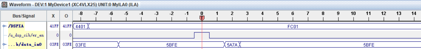

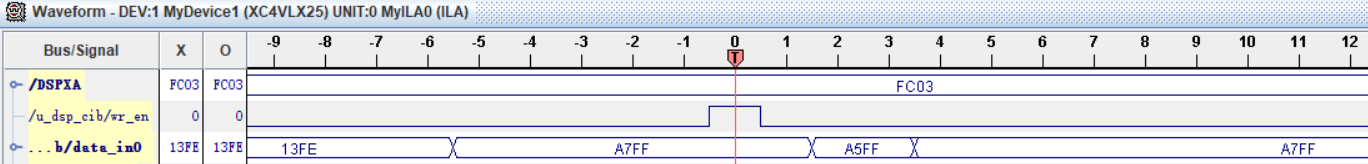
Some bits of the data is not correct, this really confuse me.
By the way, I'm using zone7 for fpga memory space, and all dsp read function works good.
Does any TI experts or other experts can help me? Thanks in advance.


