This thread has been locked.
If you have a related question, please click the "Ask a related question" button in the top right corner. The newly created question will be automatically linked to this question.
Hi Expert,
As the figure1 shown, remove R51, R53, R54 resisters from ADCINA2/1/0 pins, and connect 3V voltage with ADCINA0 & ADCINA1.
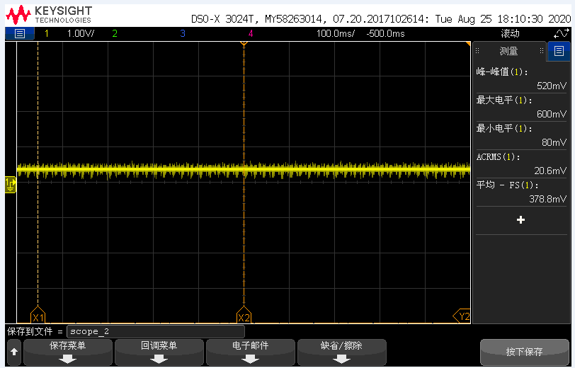
From the test result, the ADCINA2 signal is influenced by ADCINA0/1 sampling sequence.
Could you please help to explain why this happens and how to avoid this issue? Thanks!
Figure1 hardware schematic diagram
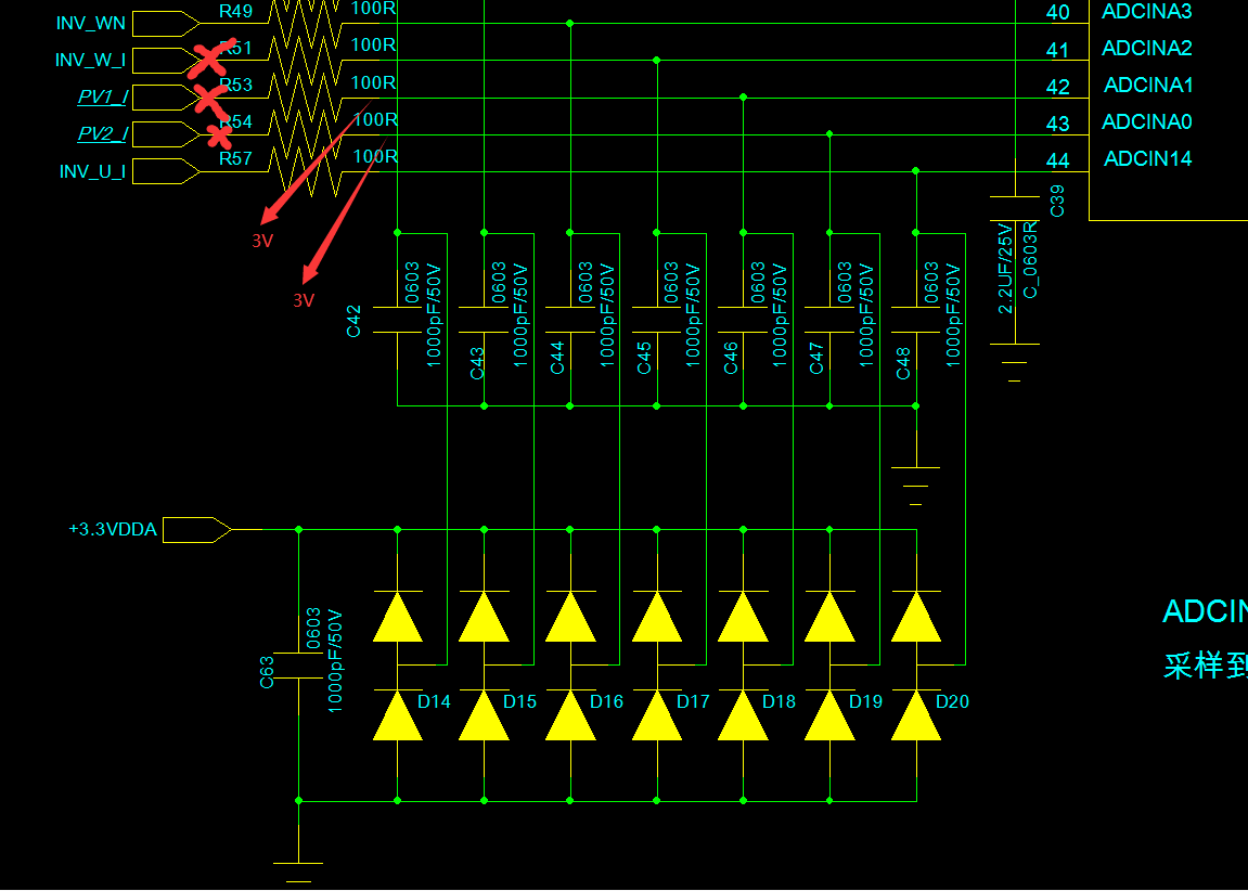
Figure2 ADC software configuration with SOC0-> ADCINA1
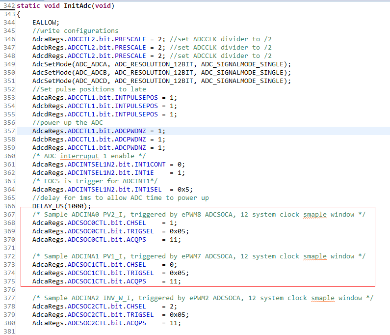
Figure3 ADCINA2 input signal with SOC0-> ADCINA1
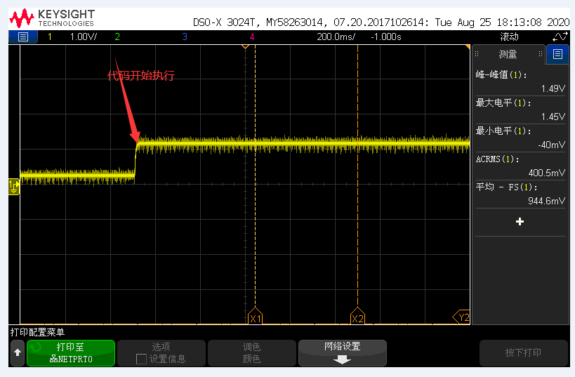
Figure4 ADC software configuration with SOC0-> ADCINA0
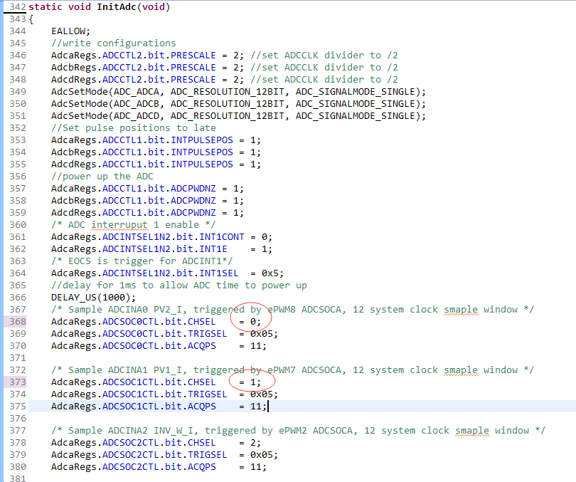
Figure5 ADCINA2 input signal with SOC0-> ADCINA0
Best Regards
Rayna
Rayna,
By design, the ADC sampling capacitor is not preconditioned to a bias voltage prior to sampling the ADC channel. This means that when a conversion is initiated, residual charge from the prior conversion will still be present on the capacitor. In the scenario that you describe, the ADCINA2 pin is floating so most of this prior charge is conducted out to the pin.
Under normal operating conditions where the ADC pin is driven, the charge carryover effect is mitigated through the combination of ACQPS selection and signal conditioning like filtering or buffering.
-Tommy
Hi Tommy,
As you said that "the ADCINA2 pin is floating so most of this prior charge is conducted out to the pin",
However the only different thing is sampling sequence, so there's a confusion that why change the sampling sequence to ADCINA0->ADCINA1->ADCINA2, there's no residual charge in ADCINA2 pin.
By the way, this issue is same whether or not floating the ADCINA2 pin.
Do you have any idea about this?
Best Regards
Rayna
Rayna,
I don't really have an idea at the moment.
Can you provide some examples with ADC conversion values?
What kind of corruption are they seeing when all of the signals are driven from the intended board signals?
-Tommy