This thread has been locked.

If you have a related question, please click the "Ask a related question" button in the top right corner. The newly created question will be automatically linked to this question.

TMS320F28377S: CMPSS Hysteresis

Part Number: TMS320F28377S


Hi

We are using the CMPSS of the TMS320F28377S

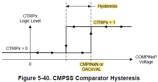
With the DAC set to 1/2 of VREF (2048) (VREF is 3.0V from VDAC pin) and an external voltage generator we measured the trip voltages, both 0-> 1 and 1->0

All voltages are in range 1.455 V +/- 10 mV

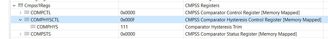
But we found that hysteresis has a value of about 3 mV, whichever value (0 to 4) we write in the COMPHYSCTL

(to do this we use the CMPSS_setHysteresis( vBase_ul, vHys_guh ) function )

The measure is done in the following way:

we use a DC voltage generator starting from 1.4V and increasing the voltage, monitoring continuously the outputs of CMPSS_getStatus( vBase_ul )

When the output goes to 1 we trace the voltage and start decreasing the voltage

We will expect an hysteresis of about 35mV (48 DAC LSB) when set to the maximum but we are not able to measure it

The behavior is the same for all CMPSS (both High and Low 

Pls, any suggestion?

By the way using a square wave and EPWM outputs we measure the time and filter response and they are as expected.

Thanks

Antonio

  • Antonio,

    DC signals from generic bench equipment tend to carry a non-negligible amount of noise when trying to measure hysteresis.  A high precision source with noise in the uV range would be recommended for a blind measurement (blind meaning that you are relying solely on the demanded voltage level of the source).  The comparator output Latch would be helpful if looking for trips using software.

    To measure hysteresis using noisier sources, you would want to use an oscilloscope for trip measurement.  Use the scope's MIN and MAX voltage measurements to determine the effective comparator input voltage level sweep.  Use the asynchronous COMPOUT path to a GPIO pin for direct observation of the comparator output -- the level is qualified as soon as the output begins to change (and most likely oscillate).

    Large amounts of bypass capacitance on the VDAC and input pin is recommended for both methods to filter out as much noise as possible.

    -Tommy

  • Hi Tommy

    Thank you for your answer and the suggestion to improve the measurements

    I will try to exec the measures and I will inform you

    Just to add some information:

    I've used an Agilent waveform generator as signal source

    To check the input voltage I read the values from the internal ADC on the same input pin: actually my software let me to continuously read the AVERAGE on 2000 samples @ 5us period. This values typically show variation on only 2 LSB  to the expected values: 1.500V means 2046 - 2048 counts on all channels with no or 1 LSB change in time (and it seems to me a very very good behavior) 

    Regarding  CMPSS setup:

    With and hysteresis of 48 LSB and DACVAL = 2048, the nominal (without offset and error calculation) threshold voltage should be:

    0 -> 1: 3V (VREFDAC) * ( 2048 + 48/2 ) / 4095  = 1.517V

    1 -> 0: 3V * ( 2048 - 48/2 ) / 4095  = 1.483V

    I mean: is hysteresis centered around nominal voltage?

    Otherwise one threshold remains at nominal value and all hysteresis is toward high (or low) voltages?

    Accessing to the COMPHYSCTL registers through emulator I noticed that there are 4 bits that can be written rather then 3 as specified on the manual

    Are the valid values from 0 to 4 as specified?

    Thanks in advance

    Antonio

  • Antonio Cattaneo said:
    To check the input voltage I read the values from the internal ADC on the same input pin: actually my software let me to continuously read the AVERAGE on 2000 samples @ 5us period. This values typically show variation on only 2 LSB  to the expected values: 1.500V means 2046 - 2048 counts on all channels with no or 1 LSB change in time (and it seems to me a very very good behavior) 

    Is this done in parallel with the trip detection?  Be careful of ADC-induced noise injection.

    Antonio Cattaneo said:
    I mean: is hysteresis centered around nominal voltage?

    There is a figure in the datasheet showing that hysteresis is applied to the 1->0 transition.

    Antonio Cattaneo said:
    Accessing to the COMPHYSCTL registers through emulator I noticed that there are 4 bits that can be written rather then 3 as specified on the manual

    Can you include a screenshot of this?  The only valid bits are COMPHYSCTL[2:0].

    Antonio Cattaneo said:
    Are the valid values from 0 to 4 as specified?

    Yes, the documentation is correct.

  • Hi Tommy

    About your questions:

    Yes the ADC acquisition is done in parallel to the trip detection

    I attach the screenshot of the COMPHYSCTL from CCS. I try to write 0xffff in the register and this is the result

    If I try to read it using 

    EALLOW;
    vHysGet_guh = HWREGH( vBase_ul + CMPSS_O_COMPHYSCTL );
    EDIS;

    in vHysGet_guh I get the value 0xf

    As you suggested I've tried to measure the trip thresholds using asynchronous COMPOUT path to a GPIO using a scope and; I stopped the ADC acquisition

    The following values are the threshold in mV with DACVAL set to half (1500mV): none calibration has been computed. With no hysteresis the output is very unstable and also in the other case I got some disturbances

    0->1   1->0

    1464  1464   COMPHYSCTL = 0
    1462  1457   COMPHYSCTL = 1
    1462  1451   COMPHYSCTL = 2
    1462  1442   COMPHYSCTL = 3
    1462  1433   COMPHYSCTL = 4

    It is exactly what I expected!

    Thanks a lot

    Antonio

  • Antonio,

    I'm glad that you were able to confirm the behavior.

    With respect to the hysteresis control bits, only COMPHYS[2:0] are functional.  COMPHYS[3] is reserved, where "reserved" can cover a wide range of implementation scenarios.  In this case, the bit was implemented in the register as writeable, but it is not controlling anything in the module.

    -Tommy