This thread has been locked.

If you have a related question, please click the "Ask a related question" button in the top right corner. The newly created question will be automatically linked to this question.

CCS/TMS320F28377D: I need help with SDFM

Part Number: TMS320F28377D
Other Parts Discussed in Thread: CONTROLSUITE, AMC1306E25, TMDSDOCK28379D, AMC1306EVM, C2000WARE, AMC1306M25

Tool/software: Code Composer Studio

I'm trying to master the SDFM of TI F28377D chip, temporarily running a single-core application (core 2 is not used). My current setup is based on the sdfm_pwm_sync_cpu01 example provided with controlSUITE, with the following adaptations:

  1. There are only SD1_D1, SD1_D2, SD1_C1 and SD1_C2 connected (GPIOs 16 to 19). Filters 2 and 
  2. The data is in Manchester encoding, therefore Sdfm_configureInputCtrl() receives MODE_2 as input.
  3. The clock, even if not required by the Manchester encoding, is supplied from one of the eCAP modules.

I have connected voltage source to the setup to emulate some kind of input for SD, and I do see some Manchester-encoded data on the corresponding DSP leg. However, running this example (or, to that matter, any sdfm example), I finish reading of the first result in the Sdfm1_ISR routine and fall to the following trap:

__interrupt void Sdfm1_ISR(void)
{
    uint32_t sdfmReadFlagRegister = 0;
    static uint16_t loopCounter1 = 0;

    //
    // Read SDFM flag register (SDIFLG)
    //
    sdfmReadFlagRegister = Sdfm_readFlagRegister(gPeripheralNumber);

    if(loopCounter1 <= MAX_SAMPLES)
    {
        //
        // Read each SDFM filter output and store it in respective filter
        // result array
        //
        Filter1_Result[loopCounter1] = SDFM1_READ_FILTER1_DATA_16BIT;
        Filter2_Result[loopCounter1] = SDFM1_READ_FILTER2_DATA_16BIT;
        Filter3_Result[loopCounter1] = SDFM1_READ_FILTER3_DATA_16BIT;
        Filter4_Result[loopCounter1++] = SDFM1_READ_FILTER4_DATA_16BIT;

        //
        // Clear SDFM flag register
        //
        Sdfm_clearFlagRegister(gPeripheralNumber,sdfmReadFlagRegister);
        sdfmReadFlagRegister = Sdfm_readFlagRegister(gPeripheralNumber);  

⇐ Here sdfmReadFlagRegister is 2147484416

        if(sdfmReadFlagRegister != 0x0)
        {
            ESTOP0;   

⇐ And, sure enough, I finish here

        }
    }

I tried disabling fiters 2, 3 and 4, to no success. What are the ways to continue from here.

  • Alexey,

    When using manchester mode (MODE = 2), SD-Cx should be left unconnected. Why have you connected ECAP module which clocks to SD-Cx? This can lead to unexpected behavior.

    When sdfmReadFlagRegister = 0x80000300, it shows modulator failure on filter1 / 2. This could be because SD-Cx is fed with input clock when it is not supposed to.

    Regards,
    Manoj
  • Thank you for the reply. I've physically cut off the clock connections, but the error remains the same. I guess, not (only) clock is responsible for it.

    There were additional questions that arose from your reply:

    Firstly, the examples provided with the controlSUITE configure PWM11 as the synchronization signal for the Sigma-Delta module 1. The same PWM11 appears in the Technical Reference Manual (SPRUHM8G). Am I required to use the PWM11? Can I route any other signal for resetting the SDFM, (for example, ECap5)? If yes, how do I configure the routing?

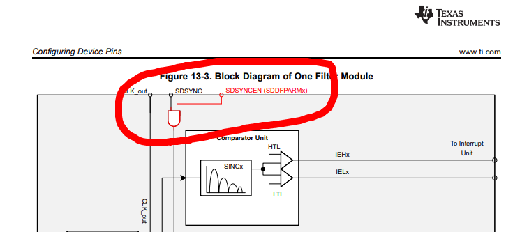
    Secondly, I'm working with Manchester encoding, and I'd like to synchronize the SDFM with an arbitrary PWM of my choise (in my case, PWM1). In the same Technical Reference Manual the scheme of synching the data filter appears "and":

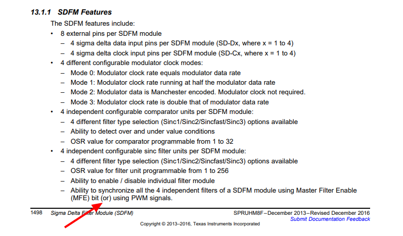
    - but in the same manual the word "or" is used in description of synchronization setup:

    What of the two options is the correct way of synchronization? Can I use only MFE bit for synchronizing SDFM?

    Thirdly, is there a way to check if the filter receives data or clock? I tried to poll the SDFM[gPeripheralNumber]->SDIFLG.bit.AF1 bit, but to no success.

    Additionally, the same scheme referenced above contains some CLK_out signal. Can I route it anywhere, and if yes, then how?

    Thanks,

    Alexey.

  • Alexey,

    1) What SD-modulator are you using? Many SD-modulators don't support manchester mode. Did you make sure your SD-modulator support manchester mode? If the SDFM (SD-Dx) doesn't receive manchester encoded bit-stream, it will report Modulator failure (MFx)

    2) It is mandatory you use PWM11 for synchronizing SDFM1. You can't use PWM1.
    PWM11.CMPC syncs SDFM1.FILTER1 & SDFM1.FILTER2
    PWM12.CMPD syncs SDFM1.FILTER3 & SDFM1.FILTER4

    Note: You don't need external connection of PWM11 to SDFM on your board to do synchronization as PWM11 has internal connection to SDFM1

    3) MFE bit can be used to synchronize using software. You can use either of the methods to perform synchronization. But, many of our customers prefer PWM method as it allows they to accurately time their events with respect to their control loop.

    Regards,
    Manoj
  • The SD modulator used in the product is TI AMC1306E25, it does support Manchester mode. According to the scope connected to the DSP GPIO 16 and 18 which were configured as Async input with MUX 7 (SD data input), exactly like the sdfm_pwm_sync_cpu01 suggests, I see the Manchester-encoded data arriving to them. I'm using only Filter 1 in my setup.

    I'll reply to this thread later, after reconfiguring my setup and re-running the tests.
  • Okay. AMC1306E25 supports IEEE 802.3-compliant Manchester encoding. SDFM expects G.E Thomas manchester encoded signal.

    It looks like AMC1306E25 Manchester encoded bit stream gives LOW to HIGH toggle pulse for a '1' and HIGH to LOW toggle pulse for a '0' whereas F28377x / F2807x seems to support HIGH to LOW pulse for a '1' and LOW To HIGH toggle for a '0'. This can be easily worked around by inverting the GPIOs inputs to SD-Dx in manchester mode.

    Please let us know if everything works as expected.

    Regards,
    Manoj
  • Well, the problem still exists.

    I've configured PWM11 as the synchronization source for SDFM. The Manchester data arrives only to GPIOs 16 and 18, i. e. to SD1_D1 and SD1_D2 only. Since the clock is not required for the SDFM working in Manchester mode, I've configured GPIOs 17 and 19 as inputs (MUX 0), and not as SD clock (MUX 7). All 4 filters are configured and enabled, but data arrives only to 2 of them.

    From the explanation above, I'd expect the corresponding MF bits in the SDIFLG register to rise. However, MF3 and MF4 bits stay at 0, and conditional breakpoint is never hit. Would you please advise on how to debug this problem?

    Additional question that still itches me is that CLK_out signal I've mentioned above (see the last question in the post with screenshots of the manual). Can I route it anywhere, and if yes, then how?

    I'm using control card TMDSDOCK28379D in my prototype.

  • Alexey,

    Lets worry about PWM11 synchronization after we resolve modulator failure (MFx) problem.

    Other questions:-

    1) Are you using PWM to clock AMC1306x?

    2) What is the behavior of PWM when emulation suspends (when hit a breakpoint)?

    3) Do you get a valid filtered data on FILTER1 and FILTER2?

    4) Does GPIO17 and 19 still receive a valid clock? (or) it is pulled high (or) low.

    CLK_out is NOT available to user, it is an internal signal. We shall be removing this CLK_out signal from the diagram to avoid such confusion.

    Regards,
    Manoj
  • Manoj,

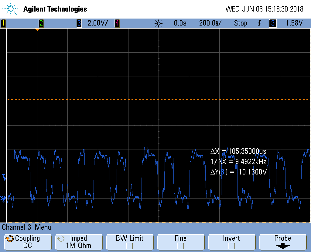
    1) I've configured ECap 5 as PWM, and am using it as clock generator (10 MHz) for the AMC1306x. SD filter receives Manchester-coded signal from the AMC1306x. SD filter clock input is not connected to any external clock. The filter receives only data, but no clock.

    For example, this Manchester-coded data stream is captured from the GPIO 16:

    2) The PWM signal (motor phase, 20 KHz) stays high or low, depending on when the breakpoint is hit. I'm using hardware breakpoints.

    3) No, there is no data on Filter1, even though the data is routed to it. Filter 2 is configured, but does not receive any data. The MFs bits are 0 on both of them. The AF bits are 0 too.

    4) The GPIOs 17 and 19 are configured as GPIO (MUX 0) and not SD clock (MUX 7). They don't receive any clock, I didn't route them. This is how I configure them:

        EALLOW;
        for(pin=16; pin<20; pin++)	// Actual SD1_C2 is 19
        {
        	GPIO_SetupPinOptions(pin, GPIO_INPUT, GPIO_ASYNC);
        	if ((pin == 17) || (pin == 19))
        		GPIO_SetupPinMux(pin, GPIO_MUX_CPU1, 0);	// GPIO
        	else
        		GPIO_SetupPinMux(pin, GPIO_MUX_CPU1, 7);	// SDFM
        }
        EDIS;

    Is it possible to get a TeamViewer or WebEX support session?

    Thanks,

    Alexey.

  • Alexey,

    I think we should still be able to resolve this issue through posts.

    I believe the clock to AMC1306x from ECAP is stopping when you hit emulator breakpoint. It is most likely root cause of the problem. When the clock to the modulator stops both modulator and SDFM wouldn't be working.

    Regards,
    Manoj
  • Manoj,

    I don't think the reason is hardware breakpoint.

    I've tried to test *SDFM[gPeripherialNumber]->SDIFLG.bits for becoming 1. Tested with AF1, AF2, and all MF* bits. Example of the code is as follows:

    void main (void) {
    
        . . . .	// Here goes all the setup
    
        for (; ; ;) {	// Main program loop
    
            if (SDFM[gPeripheralNumber]->SDIFLG.bit.AF1 != 0)
            {
                sigma_delta_read();
            }
        }
        . . . .
    }
    
    // data reading function
    void sigma_delta_read(void) {
    
        unsigned long sdfmReadFlagRegister = 0;
        static unsigned int loopCounter1 = 0;
    
        // register SDIFLG reading
        sdfmReadFlagRegister = Sdfm_readFlagRegister(1);
        Filter1_Result[loopCounter1] = SDFM1_READ_FILTER1_DATA_16BIT;
        Filter2_Result[loopCounter1] = SDFM1_READ_FILTER2_DATA_16BIT;
        Filter3_Result[loopCounter1] = SDFM1_READ_FILTER3_DATA_16BIT;
        Filter4_Result[loopCounter1] = SDFM1_READ_FILTER4_DATA_16BIT;
    
        loopCounter1 = loopCounter1 + 1;
        if (loopCounter1 == MAX_SAMPLES) loopCounter1 = 0;
    
        // clear SDIFLG register
        Sdfm_clearFlagRegister(1,sdfmReadFlagRegister);
    
        // register SDIFLG reading
        sdfmReadFlagRegister = Sdfm_readFlagRegister(1);
    }

    The breakpoint placed inside of sigma_delta_read() was never hit. Its existence did not affect the run of the program, I can see the data and the PWM still running, but the AF1 bit (in the example above) stays 0, which means that no new data exist on the SDFM. 

    Same happend with AF2, and, what troubles me most, with MF bits, even with MF3 and MF4 which are configured but physically don't receive data. The module does not detect any errors, but it also does not detect any data, even though the data streams, the GPIOs 16 and 18 are configured with GPIO_SetupPinOptions(pin, GPIO_INPUT, GPIO_ASYNC | GPIO_INVERT); (added the GPIO_INVERT flag to address the issue of inversed polarity of the data stream), and the PWM and the clock generated by ECap running. If I pause the program at a random point, the SDIFLG is 0x00000000. If I use sigma_delta_read() instead of interrupts in order to debug the program, the function is never run; if I use the interrupt, it is never fired.

    Thanks,

    Alexey.

  • Alexey,

    Looks like you are facing a basic hardware (or) software setup issue.

    Is your code working with mode0? Also, how have you configured SDFM?

    Regards,
    Manoj
  • Manoj,

    Most of the setup was copied from sdfm_pwm_sync example. The interrupts are just copy-and-paste, therefore they are not shown here.


    EALLOW; // This is needed to write to EALLOW protected registers PieVectTable.SD1_INT = &Sdfm1_ISR; // SDFM 1 PieVectTable.SD2_INT = &Sdfm2_ISR; // SDFM 2 EDIS; // This is needed to disable write to EALLOW protected registers // // Enable CPU INT5 which is connected to SDFM INT // IER |= M_INT5; // // Enable SDFM INTn in the PIE: Group 5 __interrupt 9-10 // PieCtrlRegs.PIEIER5.bit.INTx9 = 1; // SDFM1 interrupt enabled PieCtrlRegs.PIEIER5.bit.INTx10 = 1; // SDFM2 interrupt enabled Sdfm_configurePins(); // Only option1 is used here gPeripheralNumber = SDFM1; // // Input Control Module // // Configure Input Control Mode: Manchester encoded // Sdfm_configureInputCtrl(gPeripheralNumber, FILTER1, MODE_2); // Mode 0 is clk == data rate Sdfm_configureInputCtrl(gPeripheralNumber, FILTER2, MODE_2); // Mode 1 is clk == 1/2 data rate Sdfm_configureInputCtrl(gPeripheralNumber, FILTER3, MODE_2); // Mode 2 is Manchester Sdfm_configureInputCtrl(gPeripheralNumber, FILTER4, MODE_2); // Mode 3 is clk == 2 * data rate // // Comparator Module // HLT = 0x7FFF; //Over value threshold settings LLT = 0x0000; //Under value threshold settings // // Configure Comparator module's comparator filter type and comparator's OSR // value, higher threshold, lower threshold // Sdfm_configureComparator(gPeripheralNumber, FILTER1, SINC3, OSR_32, HLT, LLT); Sdfm_configureComparator(gPeripheralNumber, FILTER2, SINC3, OSR_32, HLT, LLT); Sdfm_configureComparator(gPeripheralNumber, FILTER3, SINC3, OSR_32, HLT, LLT); Sdfm_configureComparator(gPeripheralNumber, FILTER4, SINC3, OSR_32, HLT, LLT); // // Enable Master filter bit: Unless this bit is set none of the filter modules // can be enabled. All the filter modules are synchronized when master filter // bit is enabled after individual filter modules are enabled. All the filter // modules are asynchronized when master filter bit is enabled before // individual filter modules are enabled. // Sdfm_enableMFE(gPeripheralNumber); // // Data filter Module // // Configure Data filter modules filter type, OSR value and // enable / disable data filter // Sdfm_configureData_filter(gPeripheralNumber, FILTER1, FILTER_ENABLE, SINC3, OSR_256, DATA_16_BIT, SHIFT_9_BITS); Sdfm_configureData_filter(gPeripheralNumber, FILTER2, FILTER_ENABLE, SINC3, OSR_256, DATA_16_BIT, SHIFT_9_BITS); Sdfm_configureData_filter(gPeripheralNumber, FILTER3, FILTER_ENABLE, SINC3, OSR_256, DATA_16_BIT, SHIFT_9_BITS); Sdfm_configureData_filter(gPeripheralNumber, FILTER4, FILTER_ENABLE, SINC3, OSR_256, DATA_16_BIT, SHIFT_9_BITS); // // PWM11.CMPC, PWM11.CMPD, PWM12.CMPC and PWM12.CMPD signals cannot synchronize // the filters. This option is not being used in this example. // Sdfm_configureExternalreset(gPeripheralNumber, FILTER_1_EXT_RESET_ENABLE, FILTER_2_EXT_RESET_ENABLE, FILTER_3_EXT_RESET_ENABLE, FILTER_4_EXT_RESET_ENABLE); // // Init EPWMs // InitEPwm(gPWM_number); // // Enable interrupts // // Following SDFM interrupts can be enabled / disabled using this function. // Enable / disable comparator high threshold // Enable / disable comparator low threshold // Enable / disable modulator clock failure // Enable / disable filter acknowledge // Sdfm_configureInterrupt(gPeripheralNumber, FILTER1, IEH_DISABLE, IEL_DISABLE, MFIE_ENABLE, AE_ENABLE); Sdfm_configureInterrupt(gPeripheralNumber, FILTER2, IEH_DISABLE, IEL_DISABLE, MFIE_ENABLE, AE_ENABLE); Sdfm_configureInterrupt(gPeripheralNumber, FILTER3, IEH_DISABLE, IEL_DISABLE, MFIE_DISABLE, AE_DISABLE); Sdfm_configureInterrupt(gPeripheralNumber, FILTER4, IEH_DISABLE, IEL_DISABLE, MFIE_DISABLE, AE_DISABLE); <== Here I tried many ways of configuration, including enabling or disabling AE and MFIE. while((*EPWM[gPWM_number]).TBCTR < 550); // // Enable master interrupt so that any of the filter interrupts can trigger // by SDFM interrupt to CPU // Sdfm_enableMIE(gPeripheralNumber); // // Enable global Interrupts and higher priority real-time debug events: // EINT; // Enable Global interrupt INTM ERTM; // Enable Global realtime interrupt DBGM // // Setup APWM mode on CAP1, set period and compare registers <== This is clock for SD device // ECap1Regs.ECCTL2.bit.CAP_APWM = 1; // Enable APWM mode ECap1Regs.CAP1 = ECAP_TIMER_PRD; // Set Period value ECap1Regs.CAP2 = ECAP_TIMER_CMP; // Set Compare value ECap1Regs.ECCLR.all = 0x0FF; // Clear pending __interrupts ECap1Regs.ECEINT.bit.CTR_EQ_CMP = 1; // enable Compare Equal Int // // Start counters // ECap1Regs.ECCTL2.bit.TSCTRSTOP = 1; hal.tick = 0; hal.max_tick = 2480; Sdfm1Regs.SDIFLGCLR.all |= 0x00000F00; . . . . . . // // InitEPwm - Initialize specified EPWM settings // void InitEPwm(uint16_t gPWM_number) { uint16_t CMPC,CMPD; CMPC = 1250; CMPD = 1250; #ifdef CPU1 GPIO_SetupPinOptions(20, GPIO_OUTPUT, GPIO_ASYNC); // It was GPIO 0, changed it to 20 GPIO_SetupPinMux(20,GPIO_MUX_CPU1,5); // It was GPIO 0, changed it to 20 #endif EALLOW; // // Allows all users to globally synchronize all enabled ePWM modules to // the time-base clock (TBCLK) // CpuSysRegs.PCLKCR0.bit.TBCLKSYNC = 1; // // Setup TBCLK // (*EPWM[gPWM_number]).TBPHS.bit.TBPHS = 0x0000; // Phase is 0 (*EPWM[gPWM_number]).TBCTR = 0x0000; // Clear counter (*EPWM[gPWM_number]).TBPRD = EPWM_TIMER_TBPRD; // Set timer period to 2500 (*EPWM[gPWM_number]).CMPC = CMPC; // Set Compare C value (*EPWM[gPWM_number]).CMPD = CMPD; // Set Compare D value (*EPWM[gPWM_number]).CMPA.bit.CMPA = CMPC; // Set Compare C value (*EPWM[gPWM_number]).CMPB.bit.CMPB = CMPD; // Set Compare D value // // Setup counter mode // (*EPWM[gPWM_number]).TBCTL.bit.CTRMODE = TB_COUNT_UP; // Count up (*EPWM[gPWM_number]).TBCTL.bit.HSPCLKDIV = TB_DIV1; (*EPWM[gPWM_number]).TBCTL.bit.CLKDIV = TB_DIV1; // // Set actions // (*EPWM[gPWM_number]).AQCTLA.bit.CAU = 3; // Set PWM11A on event A, up // count // // Set actions // (*EPWM[gPWM_number]).AQCTLB.bit.CBU = 3; // Set PWM11A on event A, up // count EDIS; }

    I didn't try Mode 0 because it requires hardware changes, I'll be able to do it only on Sunday.

  • Alexey,

    This is strange. Given that we see a bit stream received in GPIO16 and 18. Either the SDFM filters aren't individually enabled (or) Master filter isn't enabled.

    Please send me the snapshot of memory window SDFM1 registers in memory window (or) download the contents of starting from 0x5E00 - 0x5E80?. Also, please share the contents of Sdfm_configurePins function?

    Also, can you try disabling the PWM SDSYNC feature and retry.

    Sdfm_configureExternalreset(gPeripheralNumber,FILTER_1_EXT_RESET_DISABLE,
    FILTER_2_EXT_RESET_DISABLE,
    FILTER_3_EXT_RESET_DISABLE,
    FILTER_4_EXT_RESET_DISABLE);

    Regards,
    Manoj
  • Manoj,

    When I disabled the PWM SDSYNC, the SDIFLG register became 0x80003300. Both data and failure bits of channels 1 and 2 are set.

    This is the memory window contents for SD registers wht the PWM SDSync disabled:

    Sdfm1Regs, Sdfm1Regs_SDIFLG
    3300	8000
    Sdfm1Regs_SDIFLGCLR
    0000	0000
    Sdfm1Regs_SDCTL
    2000	0000
    Sdfm1Regs_SDMFILEN
    0800	3300	0000	0000	0000	0000	0000	0000	0000	0000
    Sdfm1Regs_SDCTLPARM1
    F002
    Sdfm1Regs_SDDFPARM1
    0FFF
    Sdfm1Regs_SDIPARM1
    4800
    Sdfm1Regs_SDCMPH1
    7FFF
    Sdfm1Regs_SDCMPL1
    0000
    Sdfm1Regs_SDCPARM1
    039F
    Sdfm1Regs_SDDATA1
    0000	1969	0000	0000	0000	0000	0000	0000	0000	0000
    Sdfm1Regs_SDCTLPARM2
    F002
    Sdfm1Regs_SDDFPARM2
    0FFF
    Sdfm1Regs_SDIPARM2
    4800
    Sdfm1Regs_SDCMPH2
    7FFF
    Sdfm1Regs_SDCMPL2
    0000
    Sdfm1Regs_SDCPARM2
    039F
    Sdfm1Regs_SDDATA2
    0000	0000	0000	0000	0000	0000	0000	0000	0000	0000
    Sdfm1Regs_SDCTLPARM3
    0002
    Sdfm1Regs_SDDFPARM3
    0DFF
    Sdfm1Regs_SDIPARM3
    4800
    Sdfm1Regs_SDCMPH3
    7FFF
    Sdfm1Regs_SDCMPL3
    0000
    Sdfm1Regs_SDCPARM3
    019F
    Sdfm1Regs_SDDATA3
    0000	0000	0000	0000	0000	0000	0000	0000	0000	0000
    Sdfm1Regs_SDCTLPARM4
    0002
    Sdfm1Regs_SDDFPARM4
    0DFF
    Sdfm1Regs_SDIPARM4
    4800
    Sdfm1Regs_SDCMPH4
    7FFF
    Sdfm1Regs_SDCMPL4
    
    0000
    Sdfm1Regs_SDCPARM4
    019F
    Sdfm1Regs_SDDATA4
    0000	0000	0000	0000	0000	0000	0000	0000	0000	0000	0000	0000	0000	0000	0000	0000	0000	0000	0000	0000
    0000	0000	0000	0000	0000	0000	0000	0000	0000	0000	0000	0000	0000	0000	0000	0000	0000	0000	0000	0000
    0000	0000	0000	0000	0000	0000	0000	0000	0000	0000	0000	0000	0000	0000	0000	0000	0000	0000
    Sdfm2Regs, Sdfm2Regs_SDIFLG
    0000	0000
    Sdfm2Regs_SDIFLGCLR
    0000	0000
    Sdfm2Regs_SDCTL
    0000	0000
    Sdfm2Regs_SDMFILEN
    0000	0000	0000	0000	0000	0000	0000	0000	0000	0000
    Sdfm2Regs_SDCTLPARM1
    0000
    Sdfm2Regs_SDDFPARM1
    0000
    Sdfm2Regs_SDIPARM1
    0000
    Sdfm2Regs_SDCMPH1
    7FFF
    Sdfm2Regs_SDCMPL1
    0000
    Sdfm2Regs_SDCPARM1
    0000
    Sdfm2Regs_SDDATA1
    0000	0000	0000	0000	0000	0000	0000	0000	0000	0000
    Sdfm2Regs_SDCTLPARM2
    0000
    Sdfm2Regs_SDDFPARM2
    0000
    Sdfm2Regs_SDIPARM2
    0000
    Sdfm2Regs_SDCMPH2
    7FFF
    Sdfm2Regs_SDCMPL2
    0000
    Sdfm2Regs_SDCPARM2
    0000
    Sdfm2Regs_SDDATA2
    0000	0000	0000	0000	0000	0000	0000	0000	0000	0000
    Sdfm2Regs_SDCTLPARM3
    0000
    Sdfm2Regs_SDDFPARM3
    0000
    Sdfm2Regs_SDIPARM3
    0000
    Sdfm2Regs_SDCMPH3
    7FFF
    Sdfm2Regs_SDCMPL3
    0000
    Sdfm2Regs_SDCPARM3
    0000
    Sdfm2Regs_SDDATA3
    0000	0000	0000	0000	0000	0000	0000	0000	0000	0000
    Sdfm2Regs_SDCTLPARM4
    0000
    Sdfm2Regs_SDDFPARM4
    0000
    Sdfm2Regs_SDIPARM4
    0000
    Sdfm2Regs_SDCMPH4
    7FFF
    Sdfm2Regs_SDCMPL4
    0000
    Sdfm2Regs_SDCPARM4
    0000
    Sdfm2Regs_SDDATA4
    0000	0000	0000	0000	0000	0000	0000	0000	0000	0000

    This is the pins configuration function:

    // Sdfm_configurePins - Configure SDFM GPIOs
    //
    void Sdfm_configurePins(void)
    {


    	uint16_t pin;
    	EALLOW;
        for(pin=16; pin<20; pin++)	// Actual SD1_C2 is 19
        {
        	GPIO_SetupPinOptions(pin, GPIO_INPUT, GPIO_ASYNC | GPIO_INVERT);
        	if ((pin == 17) || (pin == 19))
        		GPIO_SetupPinMux(pin, GPIO_MUX_CPU1, 0);	// GPIO
        	else
        		GPIO_SetupPinMux(pin, GPIO_MUX_CPU1, 7);	// SDFM
        }
        EDIS;
    
        // Configure EPWM11A and B
        EALLOW;
        GpioCtrlRegs.GPAPUD.bit.GPIO20 = 1;    // Disable pull-up on GPIO20 (EPWM11A)
        GpioCtrlRegs.GPAMUX2.bit.GPIO20 = 5;   // Configure GPIO20 as EPWM11A
        GpioCtrlRegs.GPAPUD.bit.GPIO21 = 1;    // Disable pull-up on GPIO21 (EPWM11B)
        GpioCtrlRegs.GPAMUX2.bit.GPIO21 = 5;   // Configure GPIO21 as EPWM11B
        EDIS;
    
    
    }
    

    Thanks,

    Alexey.

  • Alexey,

    It is good to see the data acknowledge bit set for both filter1 and filter2.

    As I mentioned before, use are probably seeing MFx bit set because on emulation stop, your PWM / ECAP which is providing clock to SD-modulator has stopped clocking.

    Please check ECCTL1.FREE_SOFT settings? Make sure this bit (ECCTL1.FREE_SOFT) is set to either 2 (or) 3.

    Regards,
    Manoj
  • Manoj,

    After moving from Manchester encoder to another board (TI AMC1306EVM), I've successfully received the SD-data from the filter in polling mode. But several questions are still remaining:

    1) In order to perform polling, I have to register an interrupt and keep the interrupt procedure empty, otherwise the bit I'm polling on is never set.

    This is part of my main() function:

    for(;;)
    {
    	if (SDFM[gPeripheralNumber]->SDIFLG.bit.AF1 != 0)
    	{
    		sigma_delta_read();
    		SDFM[gPeripheralNumber]->SDIFLGCLR.bit.AF1 = 0;
    		}
    	}
    }

    And this is the actual data reading function:

    // data reading function
    void sigma_delta_read(void) {
    
    	unsigned long sdfmReadFlagRegister = 0;
    	static unsigned int loopCounter1 = 0;
    	Uint16 bitState = 0;
    
    	// register SDIFLG reading
    	sdfmReadFlagRegister = Sdfm_readFlagRegister(1);
    
    	Filter1_Result[loopCounter1++] = SDFM1_READ_FILTER1_DATA_16BIT;
    
    	GpioDataRegs.GPBTOGGLE.bit.GPIO62 = 1;           <==== NOTE THE TOGGLING HERE
    
    	if (loopCounter1 == MAX_SAMPLES)
    	{
    		loopCounter1 = 0;
    	}
    
    	// clear SDIFLG register
    	Sdfm_clearFlagRegister(1,sdfmReadFlagRegister);
    
    }

    I see the changes in Filter1_Result, they shift according to the change in input voltage. However, I don't know how to interpret them. When the input voltage is -0.079 mV, the reading of Filter1_Result is about 8045; when the input is 0.089 mV, the reading is about 56470, and when I unplug the input altogether (0 mV), the reading is 65030. How do I interpret the results?

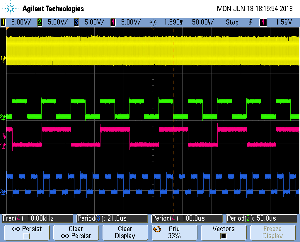
    2) This is the picture I see now on the scope:

    Green is Clock (10 MHz), Yellow is Data, Blue is PWM cycle (50 usec / 20 kHz), and blue is the toggling of the GPIO 62 that is supposed to happen upon every reading of the data. The frequency (53 usec, ~18 kHz) is insufficient; we need at least two readings during every PWM cycle, preferrably more. I understand that this is polling, and that the frequency will rise when I turn to interrupts, but it will not rise too high, since the "for" loop I copied above is the only thing DSP runs right now. What can be the suggestions for inreasing the ratio? Tweaking the OSR?

    Thanks,

    Alexey.

  • Alexey,

    1) If you want to poll for AFx bit, you can disable SDFM ePIE interrupt. That way you don't need to worry about ISR

    2) The digital value represented in filter output is the digital value corresponding to differential analog input. Digital filter output corresponding to negative differential input will be 2's complement of corresponding positive differential input.

    3) Data rate of filter output depends on OSR settings and SD-modulator sampling rate. If you want more filter data within a PWM cycle, you have to increase SD-modulator sampling freq and / or reduce OSR to increase data throughput.

    Regards,
    Manoj

  • Manoj,

    I still don't get the synchronization of SDFM. I've tried several options in order to get it, all unsuccessfully:

    1) Sdfm_configureExternalreset() was configured with FILTER_1_EXT_RESET_DISABLE. Then I tried to play with MFE bit in the following way:

    // Synchronisation routine for the SD
    __interrupt void PWM11_Comparator_C_UP_DOWN_ISR (void)
    {
    	static unsigned char sync = 0;
    	if (!sync)
    	{
    		Sdfm_enableMFE(gPeripheralNumber);
    		GpioDataRegs.GPBTOGGLE.bit.GPIO62 = 1;     // Verification GPIO toggle - just wanted to see it on the scope
    	}
    	else
    	{
    		Sdfm_disableMFE(gPeripheralNumber);
    		GpioDataRegs.GPBTOGGLE.bit.GPIO62 = 1;     // Verification GPIO toggle - just wanted to see it on the scope
    	}
    
    	// Clear INT flag for this interrupt
    	EPwm11Regs.ETCLR.bit.INT = 1;
    	// Acknowledge this interrupt to receive more interrupts from group 3
        PieCtrlRegs.PIEACK.all = PIEACK_GROUP3;
    }

    According to the Technical Reference Manual, section 13.1.1, it is possible to synchronize the SDFM module filters with Master Filter Enable bit. However, I don't see the synchronization, as I toggle another GPIO at SDFM read, and it is totally out of sync with this interrupt:

    //
    // Sdfm1_ISR - SDFM 1 ISR
    //
    __interrupt void Sdfm1_ISR(void)
    {
        uint32_t sdfmReadFlagRegister = 0;
    
        GpioDataRegs.GPFTOGGLE.bit.GPIO161 = 1;
    
        sigma_delta_read();
    
        sdfmReadFlagRegister = Sdfm_readFlagRegister(gPeripheralNumber);
        Sdfm_clearFlagRegister(gPeripheralNumber,sdfmReadFlagRegister);
    
        //
        // Acknowledge this __interrupt to receive more __interrupts from group 5
        //
        PieCtrlRegs.PIEACK.all = PIEACK_GROUP5;
    }
    

    (The function sigma_delta_read() appeared in previous posts and didn't change since then).

    Here is what I get:

    Here, yellow is raw SD data, green is PWM I'm using for synching, red is the GPIO62 that is toggled in PWM interrupt along with MFE bit, and blue is GPIO161 toggled in SD interrupt. Blue is not static, it moves, therefore it's not synchronized:

    2) I've also tried to use PWM11 C comparator for synchronization, with same results.

    3) If I enable the external reset in Sdfm_configureExternalreset(), there are no readings at all, blue line is at ground level. Looks like the reset never occurs.

    I've tried the same solution with toggling MFE bit with other PWMs, not only 11. For example, with PWM 1. I've configured the interrupt in almost the same way, also toggled a GPIO for verification. But the results were exactly the same, — there was no synchronization. The picture on the scope looked exactly as above.

    Would you please advise me on the subject? We would like to have synchronization of SD filters with PWM (assumingly, it may be achieved with MFE) and synchronization of data readings with PWM.

    The contradiction between the manual, which explicitly specifies the PWM11C as synchronization source for SDFM 1 channel 1, and the code of the examples that says "PWM11.CMPC, PWM11.CMPD, PWM12.CMPC and PWM12.CMPD signals cannot synchronize the filters" is confusing.

    Thanks,

    Alexey.

  • Alexey,

    Disabling MFE bit will disable all SDFM filter channels. Based on your question, I assume you trying to synchronize filter channels on PWM interrupt. If you are trying to synchronize SDFM filter channels on every PWM cycle, I will not recommend using MFE bit, instead use PWM11.C/D signals for SDFM1 and PWM12.C/D for SDFM2.

    We have C2000Ware example showing how to use sync SDFM filter channels using PWM11.CMPC and CMPD example. Did you already try running that

    Path: <C2000Ware>\device_support\f2837xd\examples\cpu1\sdfm_pwm_sync_cpu\

    Regards,
    Manoj
  • Manoj,

    I was attempting to synchronize the channels at least somehow. I was expecting pause in the stream of "data ready" interrupts (blue line on the scope screen image above) when PWM11.CMPC (green line) or SDFM1.MFE (red line) is 0. Scope screen images above show the contrary.

    I fully understand that disabling MFE will bring down all 4 channels of the affected SDFM, but now it doesn't sync anyway, therefore I wanted to make the things work at least through MFE bit. However, even with manipulating MFE bit the synchronization is not achieved, and I can't understand why, — this paragraph sums up section 1) of my last post.

    Of course, syncing through PWM11.CMPC would be better, but in section 2) of my last post I already wrote that it doesn't work. Even when PWM11.CMPA (which is the source for the green line on the scope screen image above) and PWM11.CMPC configured in exactly the same way, I don't see any synchronization. Do I have to make any additional configuration? Route PWM11.CMPC to SDFM somehow? AFAIK, they don't require any additional configuration, but maybe I miss something?..

    I know the sdfm_pwm_sync_cpu example. Actually, most of the code I use was taken from that example, I mentioned it several times, including the very first question of this topic. It runs but doesn't read data and doesn't sync.

    Thanks,

    Alexey.

  • Alexey,

    PWM11.CMPC / CMPD signals are internally connected to SDFM data filter and it doesn't need any external hardware connection.

    Did you try running the sdfm_pwm_sync_cpu example without any modification? If not, I would recommend you to do so.

    I don't know how you are checking filter channels are synchronized. Lets say FILTER1 / FILTER2 / FILTER3 / FILTER4 are configured the same way in SDFM1 (meaning same filter type, same OSR).

    Filter Type : Sinc3
    OSR : 256

    By setting PWM11.CMPC = PWM11.CMPD, I can synchronize all the 4 filters and all the four filters essentially restarted. SDFM achieve this by resetting the internal OSR counter to when PWM11.CMPC and CMPD signals are received. This will ensure all the four filter give new filter data at the same time instant.

    Regards,
    Manoj
  • Alexey,

    Can I close this thread? Is this issue resolved? If so, please mark the threads which help you resolve this issue.

    Regards,
    Manoj
  • Manoj,

    Actually, I've got SDFM filter mostly working. The last issue I have is two questions about the conversion of the results.

    The AMC1306EVM I use provides the output in density of 0s and 1s, with limits corresponding to -250mV being 7168 and to +250mV being 58368, according to its datasheet. SDFM comparator module of the DSP requires two numbers for the HLT and LLT being between 0 and 32768. I guess I have to divide the numbers given for AMC1306EVM by 2, receiving 3809 (0x0EE1) for LLT and 29184 (0x7200) for HLT, am I right?

    Now, the data filter gives output in ticks, which I need to convert to millivolts. On input of 0 mV I receive contstant output of 65534-65535-0, which is close to actual zero. However, on measured input of precisely 90 mV (almost noiseless, according to the scope) I receive outputs between 1385 and 1500, which are, firstly, too vague for mostly constant signal, and secondly, are way off the expected values which I suppose should be about 11000 (since 90 mV is just above the third of the positive limit which is 250 mV). 

    My current code is based on the sdfm_pwm_sync example. Mode is 0, GPIO pins 16-20 are configured as GPIO_SetupPinOptions(pin, GPIO_INPUT, GPIO_ASYNC); and GPIO_SetupPinMux(pin, GPIO_MUX_CPU1, 7);.

    Data filter is configured as:

    Sdfm_configureData_filter(gPeripheralNumber, FILTER1, FILTER_ENABLE, SINC3, OSR_256, DATA_16_BIT, SHIFT_9_BITS);

    Reading the data is performed using the macro: Filter1_Result[loopCounter1] = SDFM1_READ_FILTER1_DATA_16BIT;

  • Alexey,

    This thread already has 23 conversations.Multiple SDFM questions have been addressed. In future, please open a different thread for different question. It helps TI is housekeeping and help other people in community to easily find the answer. Can you please go ahead and mark the replies which helped answer your questions.

    Regards,
    Manoj
  • Alexey,

    For AMC1306M25
    Vclipping voltage = +/-320mv
    VIN is differential input voltage applied

    Comparator filter theoretical output = Ones_density x Max_comparatorfilter_value(FilterType, OSR)
    Data Filter theoretical output = (Ones_density-0.5)x {2x Max_digitalfilter_value(FilterType, OSR) – 1)

    For example:

    Filter Type = Sinc3
    DOSR = 256
    COSR = 32
    Vclipping = 320mv

    Max_comparatorfilter_value(Sinc3, 32) = 32767
    Max_datafilter_value(Sinc3, 256) = 16777215

    When VIN1 = 250mv
    Ones_density = (250mv + 320mv) / (2 x 320mv) = 0.8906250

    Comparator filter theoretical output = 0.8906250 x 32767 = 29183.10938 = 29183 (nearest integer)
    Data Filter theoretical output (32 bit) = (0.8906250 – 0.5) x ((2x16777215) – 1) = 13107198.83 = 13107199 (nearest integer)

    When VIN2 = 90mv
    Ones_density = (90mv + 320mv) / (2 x 320mv) = 0.640625

    Comparator filter theoretical output = 0.640625 x 32767 = 20991.35938 = 20991 (nearest integer)
    Data Filter theoretical output (32 bit) = (0.640625 – 0.5) x ((2x16777215) – 1) = 4718591.578 = 4718592 (nearest integer)

    Also, when you use PWM to synchronize the SDFM, first 2 samples after SDSYNC event is will incorrect (because filter is yet to reach steady state) for Sinc3 filter but the subsequent samples will be correct. This is expected behavior of Sinc3 filter.

    Regards,
    Manoj
  • Manoj,

    That means that, reversing the formula, Vin = Vclipping * ( 2 * Density_of_1s - 1) = Vclipping * ( 2 * ( Output_of_DF / (2 * MAX_theoretical_DF_output - 1) + 0.5) - 1) = Vclipping * (Output_of_DF / (MAX_theoretical_DF_output - 1)), right?

    However, with input of 90 mV, I still receive something like 1.21 mV. With reconfigured DF as Sinc1 (Sdfm_configureData_filter(gPeripheralNumber, FILTER1, FILTER_ENABLE, SINC1, OSR_256, DATA_16_BIT, SHIFT_0_BITS);) the output is 1.2486 mV.

    Thanks,
    Alexey.

  • Alexey,

    No, your formulae is wrong. You probably got it wrong because I didn't provide Ones_density formulae explicitly.

    Ones_density = (Vin + Vclipping) / (2 * Vclipping)

    Vin = Vclipping * { (2* Output_of_DF) / ((2*Max_digitalfilter_value(FilterType, OSR)) - 1)} --------------> Equation 1

    In your example:-

    Filter Type = Sinc1
    DOSR = 256
    Vclipping = 320mv
    Max_digitalfilter_value(Sinc1, 256) = 256


    Vin = 90mv
    Ones_density = (90mv + 320mv) / (2 x 320mv) = 0.640625


    Data Filter theoretical output = (Ones_density-0.5)x {2x Max_digitalfilter_value(FilterType, OSR) – 1)
    = (0.640625 - 0.5) x {(2*256) - 1}
    = 71.859375
    = 72 (approx)

    Using equation 1,

    Vin = 320mv * { (2 x 71.859375) /((2 x 256) - 1)}
    = 90mv

    Regards,
    Manoj
  • Manoj,

    Interesting thing happens here. Either the HW is not correct, or I copied the formula from your last reply wrong.

    With SINC1 and input of precisely 90 mV, I receive from the formula about 80 mV. With SINC3 (and appropriate formula), I get about 82 mV. When I supply 0 mV as the input, the output by both algorythms is about 1.2 mV.

    With SINC3 I can understand, the difference may be the two first data sets that may be incorrect. But SINC0 should be correct from the start. And in both cases I have OSR = 256, I guess the effect of possibly incorrect readings in SINC3 should be minimized.

    Is there a way to check the hardware? Apart from supplying +320 mV or -320 mV and verifying I receive a stable 1 or stable 0 with an occasional inverse once in 128 clocks?

    Thanks,

    Alexey.

  • Alexey,

    Are you saying your theoritical digital output calculations don't match with mine? (or) you find mismatch with practical and theoretical calculations?

    I almost get a feeling you are trying to characterize AMC1306. What exactly are you trying to do?

    Also, this thread is becoming very big. I would recommend you to open a new thread for new questions.

    Regards,
    Manoj