This thread has been locked.

If you have a related question, please click the "Ask a related question" button in the top right corner. The newly created question will be automatically linked to this question.

MSP430F5335: USCIA0, A1, B0 and B1availibility

Part Number: MSP430F5335
Other Parts Discussed in Thread: ADS1261

Dear Sirs

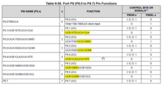
I will be using the SPI interface for my communications.  The MSP430F5335 list four SPI channels, USCIA0, A1, B0 and B1.  USCIA0 and B0 are available on P2 by port remapping and USCIA1 and B1 on P8.  However, it seems that I can use only A or B on each port but not both due to clock/chip select conflicts between A and B, (please see below).  Am I correct in this assumption?  In addition, is the STE (slave transmit enable) the same as the CS sent from the master to the slave to enable the slave?  Thank you for your time.

  • The A1CLK and B1STE (and the other combinations) do appear to conflict. [Ref User Guide (SLAU208Q) Sec 37.3.3.1 ("NOTE:")]

    I have to ask though: Do you really need the STEs? As you say, these are nominally the Chip Selects, and are pretty much required if you want to implement slave function. However, the STE function is not very useful for master mode [Ref User Guide (SLAU208Q) Sec 37.3.3.1], and a /CS GPIO can be pretty much anywhere.

  • Dear Mr. McKenney

    Thank you for your help.  After reading the suggested section more carefully, I understand the purpose of the STE signal.  I will not be using the SPI in a multi-master topology.  In other SPI implementations, I do use a GPIO for the chip select on the master side to select the desired devise.  However, when the uC is in slave mode, it seems that I need to use the STE input as a chip select.  Is this correct?  

  • You can run an SPI slave in 3-pin mode [Ref UG section 37.3.4.1, last sentence] but I expect that means that it always drives MISO, which doesn't make it a very good "bus citizen". (I haven't tried it.)

    Pointing out the obvious: SPI is designed to operate multi-drop; maybe you can combine some of the buses?

  • I'm sorry, I can see I haven't described the design properly.  I'm using the MSP430F5335 uC in an embedded sensor design.  One of the USCI SPI ports will be used as a master to control and query a TI ADS1261 ADC.  The other USCI SPI port will be a slave to the master control board, which is controlled by a TM4C1290 TIVA uC.  I know this may seem like overkill but the sensor needs to be independent of the overall system, containing its own identification and calibration data.  I hope this will help you understand what I'm trying to do.  To the point of using a 3-pin SPI, I prefer ro use the 4-pin mode.  That being said,  in section 37.3.4.1 of the user's guide, it states "In 4-pin slave mode, UCxSTE is used by the slave to enable the transmit and receive operations and is provided by the SPI master. When UCxSTE is in the slave-active state, the slave operates normally".  I have two questions; first, in my case the slave reference is the MSP430F5335 uC and the master is the M4C1290 TIVA uC.  Is this correct?  Second, the statement "When UCxSTE is in the slave-active state", refers to the signal present on the STE pin and not the state of a control resister.  Is this correct?  Thank you for your time and patients.  

  • Yes, "UCxSTE is in the slave-active state"" refers to the pin (wire) signal, not a control register. The slightly cumbersome language comes about since STE can be either active-high or active-low.(UCMODE=1 vs =2).

    It sounds as though you only need 2x SPI buses?

  • Thank you for your timely response.  This clarifies things.  You can close this issue.  Thank you again.  

**Attention** This is a public forum