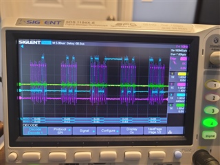
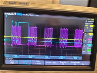
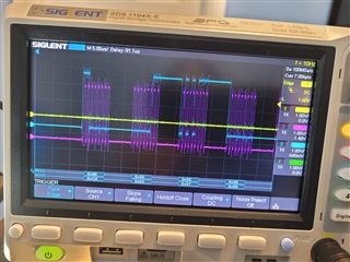
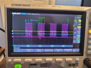
I have been able to get the correct response to the daisy chain initialization sequence using the MSP430 SPI and the MAX17841 (Table 10) connected to one MAX17853. Wake up and HELLO ALL transactions receive the correct responses on the MISO line, I get a device address that is returned as 0x001. This is the same as the Maxim evaluation GUI. These MSP430 SPI responses have been captured on the scope.
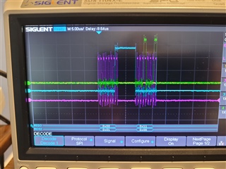
Now, I need to get Table 11 from MAX17841 working. I sent out transaction 1, 2, and 3 (WriteAll_transactions[0].Data[0] = 0xc0; WriteAll_transactions[1].Data[0] = 0xb0; WriteAll_transactions[2].Data[0] = 0x01;) but I don't get the receive of 0x12. Instead I get a 0x11 (sometimes 0x21) which means there is an RX_Overflow_Status or there is unread data. I don't understand why this is. The commands 0xC0 and 0xB0 worked fine in the transactions from Table 10. With the evaluation GUI, Table 11 works fine. So something is missing from the MSP430 handshaking. I appreciate any pointers. I have attached my current file to this post.
I tried including and removing the PEC byte from WriteAll_transactions[0] without any difference in slave response.
#include <stdio.h>
#include <stdlib.h>
#include <stdint.h>
#include <string.h>
#include <driverlib.h>
#include <intrinsics.h>
#include <msp430.h>
#include "clock~.h" // Clock configurations
#define UART_TRANSMIT_BUFFER_LENGTH 76
#define UART_TXD_PORT GPIO_PORT_P1
#define UART_TXD_PIN GPIO_PIN4
#define UART_RXD_PORT GPIO_PORT_P1
#define UART_RXD_PIN GPIO_PIN5
#define UART_SELECT_FUNCTION GPIO_PRIMARY_MODULE_FUNCTION
#define SPI_MOSI_PORT GPIO_PORT_P2
#define SPI_MOSI_PIN GPIO_PIN6
#define SPI_MISO_PORT GPIO_PORT_P2
#define SPI_MISO_PIN GPIO_PIN5
#define SPI_CLK_PORT GPIO_PORT_P2
#define SPI_CLK_PIN GPIO_PIN4
#define SPI_SELECT_FUNCTION GPIO_PRIMARY_MODULE_FUNCTION
typedef struct {
uint8_t Len;
uint8_t Data[10];
} spi_MaximTrans_t;
static uint8_t RXData[8] = {0}; //SPI receive byte
/**
* Initialize system clocks
*/
static void init_clock(void) {
// Configure one FRAM waitstate as required by the device datasheet for MCLK
// operation beyond 8MHz _before_ configuring the clock system.
FRAMCtl_configureWaitStateControl(FRAMCTL_ACCESS_TIME_CYCLES_1);
//Set DCO FLL reference = REFO
CS_initClockSignal(CS_FLLREF, CS_REFOCLK_SELECT, CS_CLOCK_DIVIDER_1);
//Set ACLK = REFO
CS_initClockSignal(CS_ACLK, CS_REFOCLK_SELECT, CS_CLOCK_DIVIDER_1);
CS_initFLLParam param = {0};
//Set Ratio/Desired MCLK Frequency, initialize DCO, save trim values
CS_initFLLCalculateTrim(CS_MCLK_DESIRED_FREQUENCY_IN_KHZ, CS_MCLK_FLLREF_RATIO, ¶m);
//Set MCLK = REFO
CS_initClockSignal(CS_MCLK, CS_REFOCLK_SELECT, CS_CLOCK_DIVIDER_1);
//Set SMCLK = DCO
CS_initClockSignal(CS_SMCLK, CS_DCOCLKDIV_SELECT, CS_CLOCK_DIVIDER_1);
//Clear all OSC fault flag
CS_clearAllOscFlagsWithTimeout(1000);
}
/**
* Initialize all of the IO pins per their configuration
*/
static void init_gpio(void) {
// Set all GPIO pins to output low to prevent floating input and reduce power consumption
GPIO_setOutputLowOnPin(GPIO_PORT_P1, GPIO_PIN_ALL8);
GPIO_setOutputLowOnPin(GPIO_PORT_P2, GPIO_PIN_ALL8);
GPIO_setOutputLowOnPin(GPIO_PORT_P3, GPIO_PIN_ALL8);
GPIO_setOutputLowOnPin(GPIO_PORT_P4, GPIO_PIN_ALL8);
GPIO_setOutputLowOnPin(GPIO_PORT_P5, GPIO_PIN_ALL8);
GPIO_setOutputLowOnPin(GPIO_PORT_P6, GPIO_PIN0 | GPIO_PIN1 | GPIO_PIN2);
GPIO_setAsOutputPin( GPIO_PORT_P1, GPIO_PIN_ALL8);
GPIO_setAsOutputPin( GPIO_PORT_P2, GPIO_PIN_ALL8);
GPIO_setAsOutputPin( GPIO_PORT_P3, GPIO_PIN_ALL8);
GPIO_setAsOutputPin( GPIO_PORT_P4, GPIO_PIN_ALL8);
GPIO_setAsOutputPin( GPIO_PORT_P5, GPIO_PIN_ALL8);
GPIO_setAsOutputPin( GPIO_PORT_P6, GPIO_PIN0 | GPIO_PIN1 | GPIO_PIN2);
}
/*
* Initialize the SPI peripheral on EUSCI A1
*/
void init_spi_peripheral()
{
GPIO_setAsPeripheralModuleFunctionOutputPin(SPI_MOSI_PORT, SPI_MOSI_PIN, SPI_SELECT_FUNCTION);
GPIO_setAsPeripheralModuleFunctionInputPin(SPI_MISO_PORT, SPI_MISO_PIN, SPI_SELECT_FUNCTION);
GPIO_setAsPeripheralModuleFunctionOutputPin(SPI_CLK_PORT, SPI_CLK_PIN, SPI_SELECT_FUNCTION);
//Initialize Master
EUSCI_A_SPI_initMasterParam param = {0};
param.selectClockSource = EUSCI_A_SPI_CLOCKSOURCE_SMCLK;
param.clockSourceFrequency = CS_getSMCLK();
param.desiredSpiClock = 1000000;
param.msbFirst = UCMSB;
param.clockPhase = EUSCI_A_SPI_PHASE_DATA_CAPTURED_ONFIRST_CHANGED_ON_NEXT;
param.clockPolarity = EUSCI_A_SPI_CLOCKPOLARITY_INACTIVITY_LOW;
param.spiMode = EUSCI_A_SPI_3PIN;
EUSCI_A_SPI_initMaster(EUSCI_A1_BASE, ¶m);
EUSCI_A_SPI_enable(EUSCI_A1_BASE);
}
void init_wd_bms_uart(void)
{
// Configure UART @38400 baud (EUSCI/16MHz)
// http://software-dl.ti.com/msp430/msp430_public_sw/mcu/msp430/MSP430BaudRateConverter/index.html
// Configure UCA0TXD and UCA0RXD
GPIO_setAsPeripheralModuleFunctionOutputPin(UART_TXD_PORT, UART_TXD_PIN, UART_SELECT_FUNCTION);
GPIO_setAsPeripheralModuleFunctionInputPin(UART_RXD_PORT, UART_RXD_PIN, UART_SELECT_FUNCTION);
EUSCI_A_UART_initParam param = {
.clockPrescalar = 26, .firstModReg = 0, .secondModReg = 214,
.selectClockSource = EUSCI_A_UART_CLOCKSOURCE_SMCLK,
.parity = EUSCI_A_UART_NO_PARITY,
.msborLsbFirst = EUSCI_A_UART_LSB_FIRST,
.numberofStopBits = EUSCI_A_UART_ONE_STOP_BIT,
.uartMode = EUSCI_A_UART_MODE,
.overSampling = EUSCI_A_UART_OVERSAMPLING_BAUDRATE_GENERATION
};
if(STATUS_FAIL == EUSCI_A_UART_init(EUSCI_A0_BASE, ¶m))
{
return;
}
EUSCI_A_UART_enable(EUSCI_A0_BASE);
}
/**
* UART_Transmit_String()
* Prints a null terminated string on the UART
* @param str null terminated string
*/
void UART_Transmit_String(const char *str)
{
int i = 0;
for(i = 0; i < UART_TRANSMIT_BUFFER_LENGTH; i++)
{
if (str[i] != '\0')
{
while (EUSCI_A_UART_queryStatusFlags(EUSCI_A0_BASE, EUSCI_A_UART_BUSY));
EUSCI_A_UART_transmitData(EUSCI_A0_BASE, str[i]);
}
else
{
break;
}
}
}
void SetUpDCInitTransactions(spi_MaximTrans_t DCInit_transactions[]){
//Enable keep alive mode
DCInit_transactions[0].Len = 2;
DCInit_transactions[0].Data[0] = 0x10;
DCInit_transactions[0].Data[1] = 0x5;
//Read Back Transaction byte
DCInit_transactions[1].Len = 2;
DCInit_transactions[1].Data[0] = 0x11;
DCInit_transactions[1].Data[1] = 0x0;
//Enable Rx Interrupt flags
DCInit_transactions[2].Len = 2;
DCInit_transactions[2].Data[0] = 0x4;
DCInit_transactions[2].Data[1] = 0x89;
//No Receive
//Read Back Transaction byte
DCInit_transactions[3].Len = 2;
DCInit_transactions[3].Data[0] = 0x5;
DCInit_transactions[3].Data[1] = 0x0;
//Clear receive buffer
DCInit_transactions[4].Len = 1;
DCInit_transactions[4].Data[0] = 0xe0;
//No Receive
//Wakeup UART slave devices
DCInit_transactions[5].Len = 2;
DCInit_transactions[5].Data[0] = 0x0e;
DCInit_transactions[5].Data[1] = 0x30;
//No Receive
//Read Back Transaction byte
DCInit_transactions[6].Len = 2;
DCInit_transactions[6].Data[0] = 0x0f;
DCInit_transactions[6].Data[1] = 0x0;
//No Receive
//2ms delay for each slave to wake up
//Wait for all UART slave devices to wake up
DCInit_transactions[7].Len = 2;
DCInit_transactions[7].Data[0] = 0x01;
DCInit_transactions[7].Data[1] = 0x0;
//Receive of 0x21 expected
//End of UART slave device wake-up period
DCInit_transactions[8].Len = 2;
DCInit_transactions[8].Data[0] = 0x0e;
DCInit_transactions[8].Data[1] = 0x10;
//Read Back Transaction byte
DCInit_transactions[9].Len = 2;
DCInit_transactions[9].Data[0] = 0x0f;
DCInit_transactions[9].Data[1] = 0x0;
//No Receive
//2ms delay for each slave to report null message
//Wait for null message to be received
DCInit_transactions[10].Len = 2;
DCInit_transactions[10].Data[0] = 0x01;
DCInit_transactions[10].Data[1] = 0x0;
//Receive 0x10 or 0x12
//Clear transmit buffer
DCInit_transactions[11].Len = 1;
DCInit_transactions[11].Data[0] = 0x20;
//No Receive
//Clear receive buffer
DCInit_transactions[12].Len = 1;
DCInit_transactions[12].Data[0] = 0xe0;
//No Receive
//Load the HELLOALL command sequence into the load queue
DCInit_transactions[13].Len = 5;
DCInit_transactions[13].Data[0] = 0xc0;
DCInit_transactions[13].Data[1] = 0x03; //message length
DCInit_transactions[13].Data[2] = 0x57; //HELLOALL command byte
DCInit_transactions[13].Data[3] = 0x0; //Register address (0x00)
DCInit_transactions[13].Data[4] = 0x0; //Initialization address of HELLOALL
//Verify contents of the load queue
DCInit_transactions[14].Len = 5;
DCInit_transactions[14].Data[0] = 0xc1;
DCInit_transactions[14].Data[1] = 0x0;
DCInit_transactions[14].Data[2] = 0x0;
DCInit_transactions[14].Data[3] = 0x0;
DCInit_transactions[14].Data[4] = 0x0;
//Transmit HELLOALL sequence
DCInit_transactions[15].Len = 1;
DCInit_transactions[15].Data[0] = 0xb0;
//No Receive
//2ms delay for each slave to respond
//Poll RX_Stop_Status Bit
DCInit_transactions[16].Len = 2;
DCInit_transactions[16].Data[0] = 0x01;
DCInit_transactions[16].Data[1] = 0x0;
//Receive 0x12
//Service receive buffer. Read the HELLOALL message that propagated through the daisy chain
//and was returned back to the ASCI.The host should verify the device count
DCInit_transactions[17].Len = 4;
DCInit_transactions[17].Data[0] = 0x93;
DCInit_transactions[17].Data[1] = 0x0;
DCInit_transactions[17].Data[2] = 0x0;
DCInit_transactions[17].Data[3] = 0x0;
//Check for receive buffer errors
DCInit_transactions[18].Len = 0x09;
DCInit_transactions[18].Data[0] = 0x0;
}
SPI_Send(spi_MaximTrans_t Transmit[], uint8_t index){
uint8_t SPI_TX_index = 0; //byte count in transaction
GPIO_setOutputLowOnPin(GPIO_PORT_P3, GPIO_PIN1); //Maxim chip select low
__delay_cycles(1000); //idle time between CS change
for(SPI_TX_index = 0; SPI_TX_index < Transmit[index].Len; SPI_TX_index++){
while(!(UCA1IFG & UCTXIFG));
UCA1TXBUF = Transmit[index].Data[SPI_TX_index];
while (!(UCA1IFG & UCRXIFG));
RXData[SPI_TX_index] = UCA1RXBUF;
}
return;
}
/**
* main.c
*/
int main(void)
{
static uint8_t TXData = 0; //transaction count
static spi_MaximTrans_t DCInit_transactions[19];
static spi_MaximTrans_t WriteAll_transactions[3];
static spi_MaximTrans_t ReadAll_transactions[3];
static uint8_t noReceive = 0;
static uint8_t noInc = 0;
char buf[76];
WDTCTL = WDTPW | WDTHOLD; // stop watchdog timer
init_clock();
init_gpio(); // Set up IO pins
GPIO_setOutputHighOnPin(GPIO_PORT_P3, GPIO_PIN1); //SPI slave chip select
// Set P1.0 to output direction
GPIO_setAsOutputPin (GPIO_PORT_P1, GPIO_PIN0);
GPIO_setAsInputPinWithPullUpResistor (GPIO_PORT_P4, GPIO_PIN2);
GPIO_enableInterrupt (GPIO_PORT_P4, GPIO_PIN2);
GPIO_selectInterruptEdge (GPIO_PORT_P4, GPIO_PIN2, GPIO_HIGH_TO_LOW_TRANSITION);
GPIO_clearInterrupt (GPIO_PORT_P4, GPIO_PIN2);
GPIO_setAsOutputPin (GPIO_PORT_P6, GPIO_PIN2);
PMM_unlockLPM5();
__enable_interrupt();
SetUpDCInitTransactions(DCInit_transactions);
TXData = 0x0; // Holds transaction number
// Setup peripheral(s) now that gpio and clocks are setup
init_spi_peripheral(); // Init Maxim spi peripheral
init_wd_bms_uart();
GPIO_setOutputHighOnPin (GPIO_PORT_P6, GPIO_PIN2); //SHDNL held high for 4ms to ensure all slaves are powered on
__delay_cycles(32000);
while (TXData < 19){
noInc = 0;
SPI_Send(DCInit_transactions, TXData);
if ((TXData == 6) || (TXData == 9) || (TXData == 15))
__delay_cycles(32000); //wait for slaves to wake up
if (TXData == 7){
if (RXData[DCInit_transactions[7].Len-1] == 0x21){
TXData++;
noReceive = 0;
noInc = 1;
sprintf(buf, "Wake Up status 0x21 received\n\r");
UART_Transmit_String(buf);
}
if (RXData[DCInit_transactions[7].Len-1] != 0x21){
TXData = 7;
noReceive++;
if (noReceive == 3){
sprintf(buf, "Wakeup Error\n\r"); //Need to set a Fault
UART_Transmit_String(buf);
}
}
}
if (TXData == 10){
if ((RXData[DCInit_transactions[10].Len-1] == 0x10) || (RXData[DCInit_transactions[10].Len-1] == 0x12)){
TXData++;
noReceive = 0;
noInc = 1;
sprintf(buf, "Wakeup Successful\n\r");
UART_Transmit_String(buf);
}
else{
TXData = 10;
noReceive++;
if (noReceive == 3){
sprintf(buf, "Wakeup Error: Preamble not received\n\r"); //Need to set a Fault
UART_Transmit_String(buf);
}
}
}
if (TXData == 16){
if ((RXData[DCInit_transactions[16].Len-1] == 0x12)){
TXData++;
noReceive = 0;
noInc = 1;
sprintf(buf, "HELLOALL successful\n\r");
UART_Transmit_String(buf);
}
else{
TXData = 16;
noReceive++;
if (noReceive == 3){
sprintf(buf, "Wakeup Error: Preamble not received\n\r"); //Need to set a Fault
UART_Transmit_String(buf);
}
}
}
if ((noReceive == 0) && !noInc){
TXData++;
}
if (TXData < 19){
GPIO_setOutputHighOnPin(GPIO_PORT_P3, GPIO_PIN1); //Maxim chip select high
__delay_cycles(1000); //idle time between CS change
}
}
GPIO_setOutputHighOnPin(GPIO_PORT_P3, GPIO_PIN1); //Maxim chip select high
__delay_cycles(1000); //idle time between CS change
//Load WRITEALL sequence into the load queue
WriteAll_transactions[0].Len = 7;
WriteAll_transactions[0].Data[0] = 0xc0; //WR_LD_Q_SPI command byte
WriteAll_transactions[0].Data[1] = 5;
WriteAll_transactions[0].Data[2] = 0x02; //WRITEALL
WriteAll_transactions[0].Data[3] = 0x12; //ADDRESS
WriteAll_transactions[0].Data[4] = 0xb1;
WriteAll_transactions[0].Data[5] = 0xb2;
WriteAll_transactions[0].Data[6] = 0Xc4; //PEC byte
// WriteAll_transactions[0].Data[7] = 0x0; //alive counter byte
SPI_Send(WriteAll_transactions, 0);
GPIO_setOutputHighOnPin(GPIO_PORT_P3, GPIO_PIN1); //Maxim chip select high
__delay_cycles(1000); //idle time between CS change
//Start transmitting the WRITEALL sequence from the transmit queue
WriteAll_transactions[1].Len = 1;
WriteAll_transactions[1].Data[0] = 0xb0; //WR_NXT_LD_Q_SPI command byte
SPI_Send(WriteAll_transactions, 1);
__delay_cycles(32000);
GPIO_setOutputHighOnPin(GPIO_PORT_P3, GPIO_PIN1); //Maxim chip select high
__delay_cycles(1000); //idle time between CS change
WriteAll_transactions[2].Len = 2;
WriteAll_transactions[2].Data[0] = 0x01; //Read RX_Status register
WriteAll_transactions[2].Data[1] = 0x0;
noReceive = 1;
while ((noReceive > 0) && (noReceive < 3)){
SPI_Send(WriteAll_transactions, 2);
if (RXData[WriteAll_transactions[2].Len-1] == 0x12){
sprintf(buf, "WRITEALL acknowledged\n\r");
UART_Transmit_String(buf);
noReceive = 0;
}
else{
noReceive++;
GPIO_setOutputHighOnPin(GPIO_PORT_P3, GPIO_PIN1); //Maxim chip select high
__delay_cycles(1000); //idle time between CS change
if (noReceive == 3){
sprintf(buf, "Writeall Error: not acknowledged\n\r"); //Need to set a Fault
UART_Transmit_String(buf);
}
}
}
GPIO_setOutputHighOnPin(GPIO_PORT_P3, GPIO_PIN1); //Maxim chip select high
__delay_cycles(1000); //idle time between CS change
ReadAll_transactions[0].Len = 7;
ReadAll_transactions[0].Data[0] = 0x93;
ReadAll_transactions[0].Data[1] = 0x0;
ReadAll_transactions[0].Data[2] = 0x0;
ReadAll_transactions[0].Data[3] = 0x0;
ReadAll_transactions[0].Data[4] = 0x0;
ReadAll_transactions[0].Data[5] = 0x0;
ReadAll_transactions[0].Data[6] = 0x0;
SPI_Send(ReadAll_transactions, 0);
GPIO_setOutputHighOnPin(GPIO_PORT_P3, GPIO_PIN1); //Maxim chip select high
__delay_cycles(1000); //idle time between CS change
ReadAll_transactions[1].Len = 2;
ReadAll_transactions[1].Data[0] = 0x09;
ReadAll_transactions[1].Data[1] = 0x0;
SPI_Send(ReadAll_transactions, 0);
GPIO_setOutputHighOnPin(GPIO_PORT_P3, GPIO_PIN1); //Maxim chip select high
__delay_cycles(1000); //idle time between CS change
}
//******************************************************************************
//
//This is the PORT2_VECTOR interrupt vector service routine
//
//******************************************************************************
#if defined(__TI_COMPILER_VERSION__) || defined(__IAR_SYSTEMS_ICC__)
#pragma vector=PORT4_VECTOR
__interrupt
#elif defined(__GNUC__)
__attribute__((interrupt(PORT2_VECTOR)))
#endif
void P4_ISR (void)
{
GPIO_clearInterrupt (GPIO_PORT_P4, GPIO_PIN2);
// Toggle P1.0 output
GPIO_toggleOutputOnPin (GPIO_PORT_P1, GPIO_PIN0);
GPIO_setOutputHighOnPin(GPIO_PORT_P3, GPIO_PIN1);
}