This thread has been locked.

If you have a related question, please click the "Ask a related question" button in the top right corner. The newly created question will be automatically linked to this question.

MSP430FR2512: I2C - Enabling slave

Part Number: MSP430FR2512

Hi,

I have a big problem with I2C communication.

Code is generated with Captivate Design Center and the initialization looks like this:

    //
    // Re-map EUSCI B0 pins to secondary locations
    // This frees up CapTIvate IOs
    //
    SYSCFG2 |= USCIBRMP;

    // P1.0: OUTPUT LOW
    // P1.1: OUTPUT LOW
    // P1.2: OUTPUT LOW
    // P1.3: OUTPUT LOW
    // P1.4: UCA0 UART TXD if (DEFAULT_OSC_SELECTION == CS_XT1CLK_SELECT), else OUTPUT LOW
    // P1.5: UCA0 UART RXD if (DEFAULT_OSC_SELECTION == CS_XT1CLK_SELECT), else OUTPUT LOW
    // P1.6: OUTPUT LOW
    // P1.7: OUTPUT LOW
#if (DEFAULT_OSC_SELECTION == CS_XT1CLK_SELECT)
    P1OUT  = (0);
    P1DIR  = (GPIO_PIN0 | GPIO_PIN1 | GPIO_PIN2 | GPIO_PIN3 | GPIO_PIN6 | GPIO_PIN7);
    P1SEL0 = (GPIO_PIN4 | GPIO_PIN5);
    P1SEL1 = (0);
#else
    P1OUT  = (0);
    P1DIR  = (GPIO_PIN0 | GPIO_PIN1 | GPIO_PIN2 | GPIO_PIN3 | GPIO_PIN4 | GPIO_PIN5 | GPIO_PIN6 | GPIO_PIN7);
    P1SEL0 = (0);
    P1SEL1 = (0);
#endif

    // P2.0: UCA0 UART TXD if (DEFAULT_OSC_SELECTION == CS_REFOCLK_SELECT), else XOUT
    // P2.1: UCA0 UART RXD if (DEFAULT_OSC_SELECTION == CS_REFOCLK_SELECT), else XIN
    // P2.2: SYNC (SET OUTPUT LOW UNLESS USED)
    // P2.3: OUTPUT LOW
    // P2.4: IRQ (OPEN DRAIN), set high to start
    // P2.5: UCB0 I2C SDA
    // P2.6: UCB0 I2C SCL
#if (DEFAULT_OSC_SELECTION == CS_XT1CLK_SELECT)
    P2OUT  =  (GPIO_PIN4);
    P2DIR  =  (GPIO_PIN2 | GPIO_PIN3 | GPIO_PIN4);
    P2SEL0 =  (0);
    P2SEL1 =  (GPIO_PIN0 | GPIO_PIN1 | GPIO_PIN5 | GPIO_PIN6);
#else
    P2OUT  =  (0);
    P2DIR  =  (GPIO_PIN2 | GPIO_PIN3 | GPIO_PIN4);
    P2SEL0 =  (GPIO_PIN0 | GPIO_PIN1);
    P2SEL1 =  (GPIO_PIN5 | GPIO_PIN6);
#endif

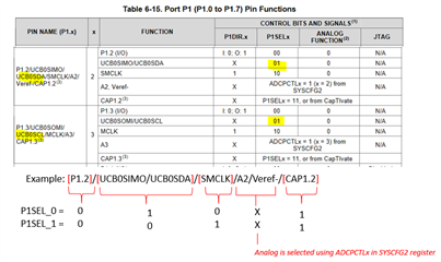
But on MSP430FR2512IPW16 there is no PIN2.5 and PIN2.6 on which the generated code set SDA and SCL.

So, I change two things:

    P1DIR  = (GPIO_PIN0 | GPIO_PIN1 | GPIO_PIN2 | GPIO_PIN3 | GPIO_PIN4 | GPIO_PIN5 | GPIO_PIN6 | GPIO_PIN7); to:

    P1DIR  = (GPIO_PIN0 | GPIO_PIN1 |  GPIO_PIN4 | GPIO_PIN5 | GPIO_PIN6 | GPIO_PIN7);

and

   P1SEL1 = (GPIO_PIN2 | GPIO_PIN3);

I also change     SYSCFG2 |= USCIBRMP  to     SYSCFG2 &= ~USCIBRMP;

I think this is what I must do if I want to get PIN1.2 = SDA  and PIN1.3 = SCL

But I still have no communication. Did I miss something?

Thank you in advance

Igor

  • Hi Igor,

    Yes, the 16-pin package does not have the secondary I2C pins as does the 20pin variant.  The only I2C on the 16-pin device is P1.2, P1.3.  Unfortunately these are also CAP1.2 and CAP1.3.

    So your configuration is correct:

    P1SEL0 = (GPIO_PIN2 | GPIO_PIN3);
    P1SEL1 = (0);
    SYSCFG2 &= ~USCIBRMP;

    If you are setting this up to communicate with the Captivate Design Center GUI, you will also need to configure one of the GPIO pins as an interrupt pin.  Most all of the Captivate demos default to P1.1.  If you choose to use this pin or another pin, make sure you configure the direction to be an input and in the CAPT_commConfig.h file you need to define the corresponding pin so the I2C driver knows which pin to drive for the interrupt.

    #define I2CSLAVE__REQ_POUT                                                (P1OUT)
    #define I2CSLAVE__REQ_PDIR                                                (P1DIR)
    #define I2CSLAVE__REQ_MASK                                                 (BIT1)

  • Hi Dennis,

    First I try with my MCU board with REGISTER_I2C, but I always get NACK response from I2C (I leave default slave address 0x0A). I also try other Salve address with no success.

    Then I try  with communication over CAPTIVATE_PGMR board to Design Center GUI with BULK_I2C (I manually trigger IRQ on PGMR board) and also get NACK

    Then I try with UART communication with Design center GUI and works perfectly.

    So I post here to see if I miss something with I2C settings.

    What else can I do?

  • Hi Igor,

    Sounds like you are doing everything ok.  Can you get a capture of the I2C transaction NACK with a scope or logic probe?  By chance do you have SDA, SCL pull up resistors on your board?  If so, what value?  Do you have any capacitors on the SDA, SCL pins? What GPIO pin are you using for the IRQ pin?

  • Hi Dennis,

    once more I update the code and now works.

    The only difference was here:

    P1SEL0 = (GPIO_PIN2 | GPIO_PIN3);

    Previously I have:

    P1SEL1 = (GPIO_PIN2 | GPIO_PIN3);

    To be honest, I have no idea what is the difference between P1SEL1  and P1SEL0

    Thank you, problem solved

    Best regards

    Igor

  • Hi Igor,

    You had me sweating there for a while. Slight smile Glad you figured it out.

    On MSP430 MCUs, each IO pin can have different functions.  On this device, up to four different functions, such as I2C, UART, PWM, ADC input, etc.  By default, they are always GPIO (general purpose input-output) at POR.

    To select a pin's "alternate" function, you set the PxSEL0 and PxSEL1 bits according to this table, which comes from section 6.11 in the datasheet.

    So to set GPIO pins P1.2 and P1.3 for I2C function you set P1SEL0 = (GPIO_PIN2 | GPIO_PIN3), and P1SEL1 = 0.

    Hope this helps explain the operation.

    At this point I'll assume you were able to move forward with your project and so I will mark this posting as RESOLVED. If this isn’t the case, please click the "This did NOT resolve my issue" button and reply to this thread with more information.
    If this thread is locked, please click the "Ask a related question" button, and in the new thread describe the current status of your issue and any additional details you may have to assist us in helping to solve your issues.

**Attention** This is a public forum