


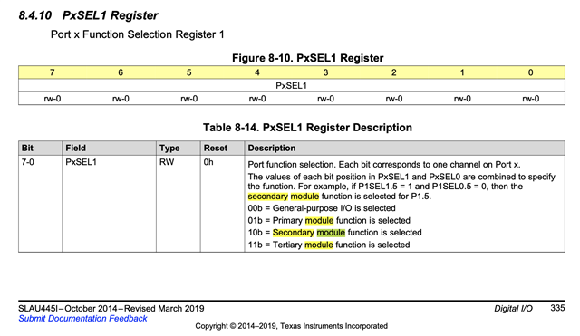
On page 335 in the MSP430 Family User Guide (SLAU445I), the order for the function selection register PxSEL1 is give as
- (00=0) GPIO
- (01=1) Primary
- (10=2) Secondary
- (11=3) Tertiary
If I look at the pin diagram and its description for P4.3 given in MSP430FR235x Datasheet (SLASEC4D), I would assume the order of pin functions are arranged accordingly:
- (00=0) GPIO = P4.3 I/O
- (01=1) Primary = UCA1TXD
- (10=2) Secondary = UCA1SIMO
- (11=3) Tertiary = ~UCA1TXD
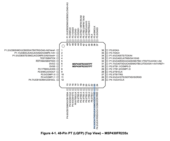
If I configure that P4.3 pin as my UART's Tx, I would of naturally thought that I should set my selector to be 01b or 11b if my logic is inverted. But then I came across page 17 on the datasheet, the PSEL is actually 01b or 10b instead. So the function selection order does not correspond to the order in the pin diagram, and instead we have this order
- (00=0) GPIO = P4.3 I/O
- (01=1) Primary = UCA1TXD
- (10=2) Secondary = ~UCA1TXD
- (11=3) Tertiary = UCA1SIMO
Where and in which documentation can I find the order of functions for a pin?
