This thread has been locked.

If you have a related question, please click the "Ask a related question" button in the top right corner. The newly created question will be automatically linked to this question.

MSP430G2231: RSA (QFN) Package ADC Inputs (P1.6 and P1.7)

Part Number: MSP430G2231

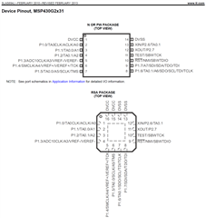
While designing around the MSP430G2231, I noticed that SLAS694J shows the N and PW (TSSOP/DIP) packages as having ADC inputs on P1.6 and P1.7, but the RSA (QFN) package is shown as NOT having ADC inputs on P1.6 and P1.7.
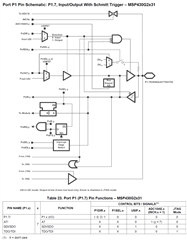
However, the port diagrams later in SLAS694J show ADC inputs on P1.6 and P1.7 and do not differentiate between the packages.  Table 1 also shows all MSP430G2231 packages as having 8 ADC channels:
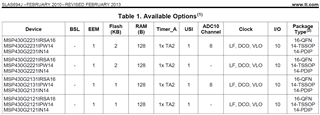
I tested a physical part in the RSA package (marking: M430G2231 TI 168G AE5L) and P1.6 and P1.7 appear to function as ADC inputs.

Are P1.6 and P1.7 in the RSA package fully-functioning ADC inputs that meet datasheet specifications?  Or should P1.6 and P1.7 NOT be used as ADC inputs on the RSA package for some undisclosed reason (out of spec, crosstalk, noise issues, etc.)?  Either way, the datasheet should be updated to make this clearer.

  • Hi TJ,

    You can see there is a note below the package: see port schematics in application information for details I/O information.

    You need to refer to that chapter for I/O function details for MSP430G2x31. In this chapter it is clear how to use each function of the I/O.

  • Hi Allen,

    Yes, I saw the note below the package:

    That information shows P1.6 and P1.7 as having ADC capabilities (as noted in my original post):

    However, if you look carefully at the pin diagram for the RSA (QFN) package, you'll notice that P1.0 through P1.5 include A0, A1,... A5, but P1.6 and P1.7 do NOT include A6 or A7:

    In contrast, the N and PW pin diagram shows A0-A7:

    That would imply that P1.6 and P1.7 on the RSA (QFN) package do not support ADC.  Yet the port schematics show that they do.  So that is why I'm asking which is correct.  It is easier to forget to add a note to the port schematics saying that P1.6 and P1.7 do not support ADC on the RSA package or forget to create separate port schematics for the RSA package than it is to remove the A6 and A7 from the pin diagram (unless A0-A5 were added and A6 and A7 were forgotten).  If the port schematics are correct for P1.6 and P1.7 and those pins function properly as A6 and A7 ADC inputs on the RSA (QFN) package, the RSA (QFN) pin diagram is incorrect and should be updated to include A6 and A7.

    Please confirm.

  • Hi TJ,

    The details of Pin function should be according to the PIN schematic. Thanks for your comments for the package information.

**Attention** This is a public forum