This thread has been locked.

If you have a related question, please click the "Ask a related question" button in the top right corner. The newly created question will be automatically linked to this question.

MSP430FR5969: I want to know the specific execution process of the instruction of MCU.

Part Number: MSP430FR5969


I want to generate a square wave using MCU. Why I don't use a timer is that its interface port cannot control the component in my design.

I use the NOP instruction to control the cycle of the square waves, the clock frequency is set to 16M, and the code is just like this:

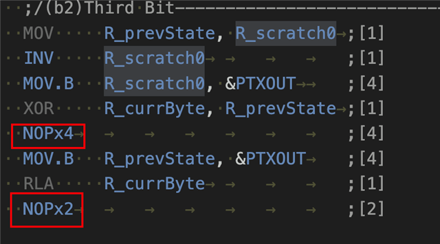
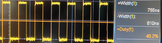
I have set the width of + and - to be equal .But the square wave is imprecise:

And I decrease one NOP number of -, the width decreased too much:

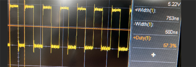
And other square wave widths are also affected.

So I want to know the specific mechanism of the instructions execution.

  • It is impossible to say what the timings will be since you haven't provided enough information. Since you state that the clock is 16MHz this implies 1 wait state. Which means that cache timing comes into play and alignment of instructions in memory is important.

    If you want to take cache timing out of the picture then you will have to lower the clock speed to 8Mhz or less and disable FRAM wait states.

  • Thanks, I have set the cache as 1 wait state and I want to use the 16MHz clock.

    So, what information can I give you to make sure what the timings will be? 

    And how can I make sure whether the instructions in memory are aligned?

  • I will not tell you the timings because they can and will vary unless you carefully align the code. The GNU assembler that I use has a .align directive for that sort of thing. Once you know the alignment then you can figure out when cache hits and misses will happen.

  • Hello, 

    a NOP is a wait state that is a jump in place instruction. Please see device User Guide for specifics. The timing of that execution and fetch are going to affected by your CPU clock frequency, and could have some variation depending on fetch timing from various parts of memory. It also can get delayed if you get an interrupt (if not turned off). For these reasons, if you need precise timing, it is recommended to use a timer. 

  • Thanks for replying. And I have said I just want to use MCU because the timer output ports (like P1.4) in the circuit board I designed don't connect the component required. 

  • I was playing a lot with code aligned on number of CPU cycles. Didn't have problems with 2xx flash family, where family datasheet have it all. With 5xx flash family things become more complicated (not covered by any TI document). And at the end found that situation with FRAM is worst.

  • Do you know how many clock cycles of one FRAM wait state?

    And can you tell me how to use the .align? I added it in my code but it had no effect.

  • Thank you very much. I feel annoyed that when I change few of the code, I should rethink and adjust the code to align.

    Do you have any good way?

  • A FRAM wait state is just what it says. One extra MCLK cycle.

    The documentation for the GNU assembler provides all the detail on how to use .align. Which shows that if you just plopped in ".align" you got nothing because you didn't provide the argument describing the alignment. If you are using this with the C inline assembly syntax you had better include a NOP as the fill value.

**Attention** This is a public forum