This thread has been locked.

If you have a related question, please click the "Ask a related question" button in the top right corner. The newly created question will be automatically linked to this question.

MSP430F5326: SPI slave timing issue

Part Number: MSP430F5326


Compiler: IAR 4.21.6

The SPI is set up as slave. Master clock is 312.5 kHz

Observation:

The MISO line is not synchronized to the rising edge of the clock input.

This can rarely happen right after a power-on-reset. It may also rarely happen during longer runtime of the software (several hours).

Most of the time everything works according to SPI spec and without any problems.

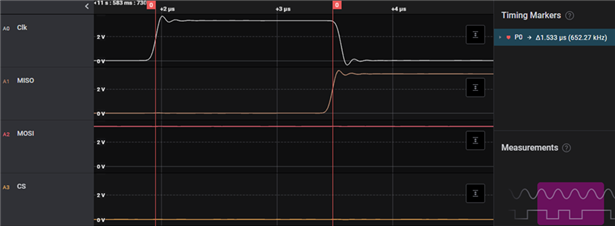
Logic analyzer recordings:

In the event of the described error, a delay can be observed between the rising edge of the clock line and the change in the data line (MISO).

This delay increases during runtime until the data change of the MISO line and the falling edge of the clock line happen at the same moment.

When this happens, the master is no longer able to correctly interpret the transmitted data.

Communication right after reset:

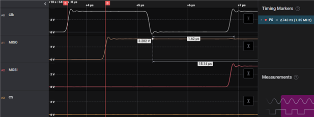
Right after reset, there is already a delay of ~750ns observable. The MISO line should change its output with the rising edge.

Miso timing shifts:

300 ms after the reset, the data line change shifted further towards the falling edge of the clock.

Last “successful” communication:

1.04 seconds after the reset, the data line change is almost coincident to the falling edge of the clock line.

How is it possible that the SPI unit of the processor behaves this way?

  • Hi Benjamin,

    Just a couple questions to help narrow down the source.

    Can you share the code section you are using when you initialize the SPI peripheral and the SPI ISR? This will let me verify that the peripheral is being initialized correctly.

    Do you have any passive components on the SPI lines or is it a direct connection between both devices?

    Are you using the DMA with the SPI?

    Regards,

    Luke

  • Hi Luke,

    thank you for your quick reply.

    DMA is not used. It is purely handled by interrupt routines on byte level.

    The hardware setup is as following:
    100 Ohm on the MISO line to the master.
    uClamp0504A from CS, MOSI, MISO and Clk to GND.

    SPI peripheral initialization code:

    void SPI_InitUsciA0asSpi(void)
    {
        UCA0CTL1 = UCSWRST;
        UCA0CTL0 = UCMSB + UCMODE1 + UCSYNC; // MSB first, 8Bit, 4 Pin SPI active low, Slave, Output at rising edge
    
        P3SEL |= (BIT2 + BIT3 + BIT4);  // SPI functionality
        P3DIR |= BIT4;
        P3DIR &= ~BIT2;
        P3DIR &= ~BIT3;
    
        P2SEL |= BIT7;  // P2.7 with SPI functionality
        P2DIR &= ~BIT7;
    
        UCA0CTL1 &= ~UCSWRST;   // Clear Software reset bit (enables USCI_A0)
        UCA0IE = UCRXIE;  // Recieve interrupt enable
    }

    SPI Interrupt Handling code:

    #define HW_SetCpuToFullSpeedMode()         UCSCTL5 &= 0xFFF8
    #define HW_SetCpuToLowSpeedMode()          {UCSCTL5 &= 0xFFF8;UCSCTL5 |= 0x0002;}
    
    // Clear Interrupt Flags and enable Transmit interrupt
    inline void SPI_EnableTransmitInterrupt(void)
    {
      UCA0IFG = 0;  // Clear Interrupt Flags
      UCA0IE = UCTXIE;  // Transmit interrupt enable
    }
    
    
    // Read Transmit buffer
    inline unsigned char SPI_ReadTransmitBuffer(void)
    {
      return UCA0TXBUF;
    }
    
    #pragma vector=USCI_A0_VECTOR
    __interrupt void ISR_UsciA0 (void)
    {
      timeoutInt = 0;
      SPI_SpiCommStateMachine(UCA0RXBUF);   // erstes byte 5us bei 20Mhz
    }
    
    // SPI Comunication State Machine
    #pragma inline=forced
    inline void SPI_SpiCommStateMachine(unsigned char recByte)
    {
      static unsigned char checkSum = 0;
      static unsigned char checkSumError = 0;
      
      switch(commState)
      {
        case 0:   // Command Byte
    
          if (P2IFG&BIT2)  
            HW_SetCpuToFullSpeedMode();
    
          SPI_SpiCommInterpreter(recByte);
          HW_SetNewTimerA0cc1Value();         // for timeout start timer
          TA0CCTL1_bit.CCIFG = 0;             
          HW_EnableTimerA0IcOc1_Interrupt();  
          checkSum = recByte;
          break;
    
        case 1:  // Receive Bytes from Master
          *spiRecievePtr = recByte;
          spiRecievePtr++;
          checkSum += recByte;
          spiRecieveDataLenght--;
          if(spiRecieveDataLenght == 0)
          {
            commState = 2;
          }
          break;
    
        case 2: // Get Checksum from Master and send 1st Byte
          SPI_EnableTransmitInterrupt();  // Change to transmit interrupt
          recByte = ~recByte;
          if(checkSum != recByte) // Checksum Error (Invertierte Checksum)
          {
            checkSumError = 1;
            spiStatus.bit.commandRecieved = 0;
          }
          else
          {
            checkSumError = 0;
          }
          checkSum = SPI_ReadTransmitBuffer();
          if(spiTransmitDataLenght == 0)
          {
            commState = 4;
          }
          else
          {
            commState = 3;
          }
          break;
    
        case 3: // Send bytes to Master
          SPI_WriteTransmitBuffer(*spiTransmitPtr);
          checkSum += *spiTransmitPtr;
          spiTransmitPtr++;
          spiTransmitDataLenght--;
          if(spiTransmitDataLenght == 0)
          {
            commState = 4;
          }
          break;
    
        case 4: // Send Checksum to Master (Invertierte Checksum)
          SPI_WriteTransmitBuffer(~(checkSum + checkSumError));
          commState = 5;
          break;
    
        case 5: // Letztes Byte
          SPI_WriteTransmitBuffer(0);
          SPI_EnableRecieveInterrupt();
          commState = 0xFF;
          break;
    
        case 10: //undefined command wait until end
          SPI_EnableTransmitInterrupt();  // Change to transmit interrupt
          SPI_WriteTransmitBuffer(0);
          // wait for timeout 6ms
          break;
    
        default:    // Letztes Byte wurde Empfangen
          HW_DisableTimerA0IcOc1_Interrupt(); // Timeout Counter deaktivieren
          SPI_WriteTransmitBuffer(0);
          UCA0IFG = 0;  // Clear Interrupt Flags
          commState = 0;
          if(spiStatus.bit.inertDataSending)
          {
            spiStatus.bit.inertDataSending = 0;
            spiStatus.bit.inertDataSent = 1;
            errorState.bit.WdgResetOccured = 0; // Clear Watchdog Error
          }
          if(checkSumError)
          {
            ResetRequired = 0;
            spiStatus.bit.chkSumErr = 1;
            checkSumError = 0;
          }
          else if(spiStatus.bit.commandRecieved)
          {
            spiStatus.bit.commandPending = 1;
          }
          spiStatus.bit.commandRecieved = 0;
          if(clrCommErrors)
          {
            SPI_ResetCommErrors();
            errorState.bit.WdgResetOccured = 0; // Clear Watchdog Error
            clrCommErrors = 0;
          }
          if(cpuLowFreqMode)
          {
            HW_SetCpuToLowSpeedMode();
          }
          break;
      }
    }

    Regards,

      Benjamin

  • The clamp diodes seem pretty useless since the voltage they clamp to is greater than the voltage at which the MSP430 internal clamp diodes will be turned on. They also add a fair amount of capacitance.

    Your SPI code has a race condition. After receiving the checksum byte it enables the transmit interrupt. Since TXIFG is set, this queues up an immediate interrupt. Will the ISR return and the next ISR get to the point where it puts data into TXBUF before it is needed? It seems unlikely  since worst case you only have half a SPI clock period to do all that work. Which means that the first byte transmitted will be whatever was hanging out in TXBUF.

    But not going to effect data out timing. You show the data out timing shifting slowly from the rising edge to the falling edge. Does it stop there? Does this vary with SPI clock frequency? In other words does the shift stop at the falling edge or does the delay increase continuously?

  • Thanks for the commentary regarding the clamp diodes. I will talk to the electronics team about the necessity of such diodes.
    However, the rise and fall times of all slopes look fine.

    I am aware of this race condition. This isn't pretty, but the first byte of the transmition has no meaning for the master.

    After the data out of the MOSI line reaches the falling edge of the CLK, all further data transmitted is zero.
    In my oppinion, this happens because of the default section, or case 10, of the switch case.
    It seems the slave is no longer capable of understanding the incomming commands an therefore reacts with zeros.
    So I'm no longer capable of observing edges since zero contains no edges.

    The slave does not recover from this state. The communication continues with zeros only.

    I also tried to communicate with half baudrate. This didn't solve the problem either.
    Unfortunately I have no recording of the half baudrate try.

    Correct me if I'm wrong, but the SPI slave is internally implemented via a shift register that is clocked via the CLK by the master.
    How is it even hardware-wise possible that the MISO edge shifts over time?

  • Hi Benjamin,

    Hard-ware wise there is not a reason that this delay is propagating until it reaches the falling edge.

    I do see some code stuff that could be causing this delay.

    1. The ISR is very generic and it is receiving any SPI interrupt so not dependent on a TX or RX flag
    2. There is a lot of code in the ISR
      1. This can cause delays as you are changing things inside of a particularly fast communication (especially the default section)
    3. I don't see how you ever get out of State 10, maybe this is intentional but I would do some check so you can see when you are in that state.
    4. See the SPI example for the peripheral (slave) side. SPI Example

    Regards,

    Luke

  • Point 1 and 2:
    I get the idea behind your answer, but I don't understand how that should cause such a problem.
    If the interrupt processing takes too long, the only thing that can happen is that entire bytes are missing.
    I don't understand how this can alter the bit timing that is controlled by the external CLK source.

    Point 3:
    State 10 is left via a hardware timer that resets the SPI to its initial state.

    If I would be able to better understand the internal structure of the SPI unit of the procesor, I could maybe narrow down the source of the problem.

    Is there any kind of documentation giving a more detailed insight into the SPI unit?

    Regards,
       Benjamin

  • More detailed insight into the operation of the SPI port would require a detailed description of the hardware. Something like VHDL source for the hardware design. But that will never happen. In any case I cannot think of anything that would cause it to change its operation gradually from the rising edge to the falling edge.

    Use of the hardware in slave mode is going to be far less common so it is possible that you have found a problem within the MSP430. But it isn't likely.

    Your ISR is still deeply flawed. I didn't realize that at first because it obfuscates some things. I didn't notice that you clear the interrupt flags before enabling the transmit interrupt. This is really bad.

  • Hi Ben,

    Besides the Datasheet and the User's Guide there won't be additional information on the SPI peripheral. 

    Further on point 2, you still have the SPI transmit in the ISR so the SPI interrupt would queue for a send even if the timing is off, I think what eventually happens is you get out of the proper phase and polarity alignments.

    Is it possible to bring out most of the code from the ISR and put it into main, check states in the main and then send the SPI transmit event and process it similar to our example?

    Regards,

    Luke

  • I don't think that the timing of writes to TXBUF are going to do much to the bit timing. This of course depends on the timing of the transfer of data from TXBUF to the transmit shift register. In slave mode, all that is available is the externally applied SPI clock.

    I suppose it is possible that there is some undocumented state machine within the SPI port that runs off of an internal clock. In which case setting UCSSEL to something other than the reserved setting might help.

**Attention** This is a public forum