Part Number: CC430F5137
Other Parts Discussed in Thread: TEST2
Hi,
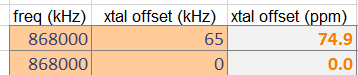
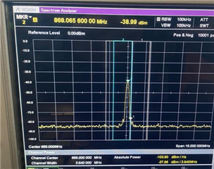
We manufacture low power consumption devices using the CC430F5137 product. We have 2 devices communicating with each other.The receiver responds to the signal sent by the transmitter.Sometimes the transmitter sends signals and we observe that the receiver is not responding .When we watched the signal in the RF spectrum device, we observed that it was broadcasting as 868,065 Mhz instead of 868 Mhz. We're investigating the possibility that this shift could cause the error.
I sent you the screen of the spectrum device.
I give below the RFsetting register values of the receiver and transmitter.
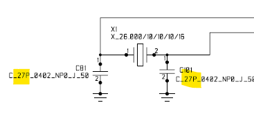
We use “ECS-260-18-30BQ-DS” as crystal. We are waiting for your opinions about our crystal selection.
I look forward to your suggestions for solutions.
Thank you.
RF_SETTINGS rfSettings = {
0x08, // FSCTRL1 Frequency synthesizer control.
0x00, // FSCTRL0 Frequency synthesizer control.
0x21, // FREQ2 Frequency control word, high byte.
0x62, // FREQ1 Frequency control word, middle byte.
0x76, // FREQ0 Frequency control word, low byte.
0x9A, // MDMCFG4 Modem configuration.
0x83, // MDMCFG3 Modem configuration.
0x93, // MDMCFG2 Modem configuration.
0x22, // MDMCFG1 Modem configuration.
0xF8, // MDMCFG0 Modem configuration.
0x00, // CHANNR Channel number.
0x34, // DEVIATN Modem deviation setting (when FSK modulation is enabled).*35
0x56, // FREND1 Front end RX configuration.
0x10, // FREND0 Front end TX configuration.
0x10, // MCSM0 Main Radio Control State Machine configuration.*10
0x16, // FOCCFG Frequency Offset Compensation Configuration.
0x6C, // BSCFG Bit synchronization Configuration.
0x43, // AGCCTRL2 AGC control.
0x40, // AGCCTRL1 AGC control.
0x91, // AGCCTRL0 AGC control.
0xE9, // FSCAL3 Frequency synthesizer calibration.
0x2A, // FSCAL2 Frequency synthesizer calibration.
0x00, // FSCAL1 Frequency synthesizer calibration.
0x1F, // FSCAL0 Frequency synthesizer calibration.
0x59, // FSTEST Frequency synthesizer calibration.
0x81, // TEST2 Various test settings.
0x35, // TEST1 Various test settings.
0x09, // TEST0 Various test settings.
0x47, // FIFOTHR RXFIFO and TXFIFO thresholds.
0x2E, // IOCFG2 GDO2 output pin configuration.
0x2E, // IOCFG0 GDO0 output pin configuration. Refer to SmartRF® Studio User Manual for detailed pseudo register explanation.
0x04, // PKTCTRL1 Packet automation control.
0x04, // PKTCTRL0 Packet automation control.*
0x00, // ADDR Device address.
0x18 // PKTLEN Packet length.
};