Part Number: EVM430-FR6043
Other Parts Discussed in Thread: MSP430FR6043, , TIDM-02003
Greetings,
We're trying to communicate our EVM430-FR6043 with an Arduino mega 2560 via SPI (using a 5V-3.3V level shifter). The MSP430FR6043 is intended to work as slave, while the Arduino acts as master. But we're having issues making it work. The eUSCI module simply doesn't seem to work: we're not getting any exceptions on the IDE, the rest of the code is working properly, we don't measure any signals on MISO, the eSUCI_A receive interrupts, although enabled, are not occurring even though we're transmitting data from the Arduino to the MSP.
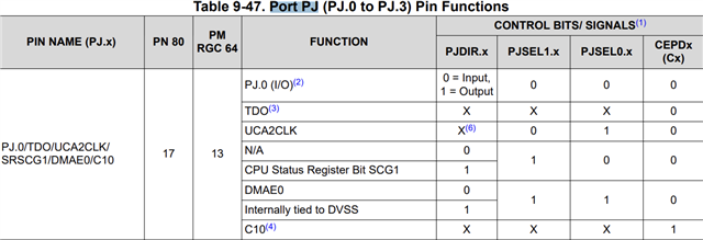
From what we've seen on the TIDM-02003 schematic, it seems the only eUSCI_A module available is eUSCI_A2, which is multiplexed to pins 0,1,2 & 3 of Port J. These are connected to the BoosterPack pin headers (J7 & J8) as shown on the schematic:
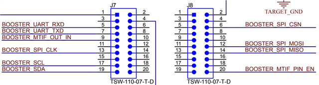
We've also set J30 in order to use pin 1 of J7 as VCC for the level shifter.
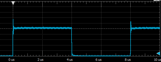
From what we've seen, all connections are correct. We've measured the voltage on the pins of the MSP430FR6043 and we've seen that the signals are correct. For example, in this image the blue signal is the clock outputted by the arduino that is connected to the corresponding pin on the MSP:

This seems to imply that this is an issue on our code. We based our code on the SPI slave example for the eUSCI_A module of the Driver library. Here is our code (some parts were commented for debugging):
#include <msp430.h>
#include <eusci_a_spi.h>
#include <gpio.h>
#include <Communications.h>
#include <stdbool.h>
#include <stdint.h>
CommunicationStatus com_status;
void Communications_setup(void){
WDT_A_hold(WDT_A_BASE);
/* 1. Configure pins for eUSCI_A2:
* Change Peripheral Module Function of pins 0,1,2,3,4,5 of PORT J to use eUSCI_A2 instead
* - Set PIN 0 as Input (CLK)
* - Set PIN 1 as Input (STE) (Unused)
* - Set PIN 2 as Input (MOSI)
* - Set PIN 3 as Output (MISO)
*/
GPIO_setAsOutputPin(GPIO_PORT_PJ, GPIO_PIN3);
GPIO_setAsInputPin(GPIO_PORT_PJ, GPIO_PIN0 + GPIO_PIN1 + GPIO_PIN2);
GPIO_setAsPeripheralModuleFunctionInputPin(
GPIO_PORT_PJ,
GPIO_PIN4 + GPIO_PIN5,
GPIO_PRIMARY_MODULE_FUNCTION
);
GPIO_setAsPeripheralModuleFunctionInputPin(
GPIO_PORT_PJ,
GPIO_PIN0 + GPIO_PIN1 + GPIO_PIN2,
GPIO_SECONDARY_MODULE_FUNCTION
);
GPIO_setAsPeripheralModuleFunctionOutputPin(
GPIO_PORT_PJ,
GPIO_PIN3,
GPIO_SECONDARY_MODULE_FUNCTION
);
//2. Configure GPIO for slave select:
GPIO_setAsInputPinWithPullDownResistor(
GPIO_PORT_P2,
GPIO_PIN2
);
GPIO_enableInterrupt(
GPIO_PORT_P2,
GPIO_PIN2
);
/*
* 3. Disable the GPIO power-on default high-impedance mode to activate
* previously configured port settings
*/
PMM_unlockLPM5();
// 4. Initialize eUSCI module in SPI slave mode:
EUSCI_A_SPI_initSlaveParam params = {0};
// The following parameters are set by default:
params.msbFirst = EUSCI_A_SPI_MSB_FIRST;
params.clockPhase = EUSCI_A_SPI_PHASE_DATA_CHANGED_ONFIRST_CAPTURED_ON_NEXT;
params.clockPolarity = EUSCI_A_SPI_CLOCKPOLARITY_INACTIVITY_LOW;
params.spiMode = EUSCI_A_SPI_3PIN;
EUSCI_A_SPI_initSlave(EUSCI_A2_BASE, ¶ms);
// 5. Start eUSCI_A2 module:
EUSCI_A_SPI_enable(EUSCI_A2_BASE);
// 6. Enable Interrupt & clear flags (just in case)
EUSCI_A_SPI_clearInterrupt(EUSCI_A2_BASE,EUSCI_A_SPI_TRANSMIT_INTERRUPT);
EUSCI_A_SPI_enableInterrupt(
EUSCI_A2_BASE,
EUSCI_A_SPI_TRANSMIT_INTERRUPT + EUSCI_A_SPI_RECEIVE_INTERRUPT
);
//__bis_SR_register(GIE);
}
void Communications_send(uint8_t transmit_data){
EUSCI_A_SPI_transmitData(EUSCI_A2_BASE, transmit_data);
}
#if defined(__TI_COMPILER_VERSION__) || defined(__IAR_SYSTEMS_ICC__)
#pragma vector = PORT2_VECTOR
__interrupt void Port2_ISR (void)
#elif defined(__GNUC__)
void __attribute__ ((interrupt(PORT2_VECTOR))) Port2_ISR (void)
#else
#error Compiler not supported!
#endif
{
switch(GPIO_getInputPinValue(GPIO_PORT_P2, GPIO_PIN2)){
case GPIO_INPUT_PIN_LOW:
com_status = COMMUNICATION_STATUS_ACTIVE;
break;
/* case GPIO_INPUT_PIN_HIGH:
com_status = COMMUNICATION_STATUS_INACTIVE;
EUSCI_A_SPI_disableInterrupt(
EUSCI_A2_BASE,
EUSCI_A_SPI_RECEIVE_INTERRUPT
);
break;*/
}
GPIO_clearInterrupt(GPIO_PORT_P2,GPIO_PIN2);
//__bis_SR_register(LPM0_bits + GIE);
}
#if defined(__TI_COMPILER_VERSION__) || defined(__IAR_SYSTEMS_ICC__)
#pragma vector=USCI_A2_VECTOR
__interrupt void USCI_A2_ISR (void)
#elif defined(__GNUC__)
void __attribute__ ((interrupt(EUSCI_A2_VECTOR))) USCI_A2_ISR (void)
#else
#error Compiler not supported!
#endif
{
switch(__even_in_range(UCA2IV, USCI_SPI_UCTXIFG))
{
case USCI_SPI_UCRXIFG: // UCRXIFG
//USCI_A0 TX buffer ready?
while (!EUSCI_A_SPI_getInterruptStatus(EUSCI_A2_BASE,
EUSCI_A_SPI_TRANSMIT_INTERRUPT
));
//Transmit data to master
EUSCI_A_SPI_transmitData(EUSCI_A2_BASE,
13
);
//Receive data from master
uint8_t receiveData = EUSCI_A_SPI_receiveData(EUSCI_A2_BASE);
break;
default:
break;
}
}
bool Communications_isActive(){
if (com_status == COMMUNICATION_STATUS_ACTIVE) {
return true;
}else{
return false;
}
}
uint8_t Communications_read(){
return EUSCI_A_SPI_receiveData(EUSCI_A2_BASE);
}
int main(void)
{
Communications_setup();
while(1){
Communications_send(13);
__delay_cycles(500);
}
}
Our guess is that, for some reason, the eUSCI_A2 module isn't receiving the clock signal from the Arduino, but we don't know how to confirm this as we can't see UCxCLK.
Checking the EVM schematic once again we found that pin 17 on the MSP430, which is multiplexed to PORTJ.0 and is connected to the BOOSTER_SPI_CLK pin on J7, is labeled as UAC2CLK instead of UCA2CLK:
At first we thought this was simply a typo, as we didn't find any other pin with a similar name and it seems from the datasheet that this pin is indeed connected to the CLK of the eUSCI_A2 module.
We'd like to know if it is possible to verifiy if clock is being read by the eUSCI module, or what could be the issue here that is causing this behavior.
Thanks a lot in advance.
EDIT: We're using the ezFET programming & debugging circuit incorporated on the board