This thread has been locked.

If you have a related question, please click the "Ask a related question" button in the top right corner. The newly created question will be automatically linked to this question.

MSP430F5172: Interleaved PWM Overlapping High When Timer D0 Begins

Part Number: MSP430F5172
Other Parts Discussed in Thread: CCSTUDIO

Hi,

I am using an MSP430F5172 to create an interleaved PWM on Timer D0 with CCR1 and CCR2. D0 is running in up/down mode and CCR1/2 are operating in compare mode toggle-reset and toggle-set respectively.

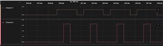
The PWMs are being staggered correctly; however, there is an issue on the first pulse when the timer kicks off where it has both outputs high at the same time, which is a scenario we are trying avoid.

Below is an image of the signals where D0.1 is TD0 CCR1 and D0.2 is TD0 CCR2.

When analyzing these signals in TI's CCStudio example code tutorials, this phenomena also occurs. Is there a way around this? Is there a latent configuration issue?

TI's documentation states that this PWM setup is perfect for scenarios where both signals shouldn't be high at the same time, but this start-up behavior defeats the purpose... which makes me think I have a configuration issue.

Below is the setup code.

void init_timers(void)
{
    struct s_TLV_Timer_D_Cal_Data * pTD0CAL;  // Structure initialized in tlv.h
    uint8_t bTD0CAL_bytes;

    // Stop WDT
    WDT_A_hold(WDT_A_BASE);

    //Get TimerD0 Cal Values (instance 0)
    TLV_getInfo(TLV_TAG_TIMER_D_CAL, 0, &bTD0CAL_bytes, (uint16_t **) &pTD0CAL);

    if(bTD0CAL_bytes == 0x0)
    {
      // No TimerD free running cal data found
      while(1);                             // Loop here
    }

    /*
    * Configuration
    */
    // Setup TD0
    TD0CTL0 |= TDCLGRP_0 | CNTL_0 | TDSSEL_2 | MC__UPDOWN | ID_0 | TDCLR;
    TD0CTL1 |= TDIDEX_0  | TDCLKM_1;

    // Enable high resolution clock
    TD0HCTL0 = TDHEN + TDHM_1;
    TD0HCTL1 = pTD0CAL->TDH0CTL1_128;

    // Configure CCR modes
    TD0CCTL0 |= TIMER_D_OUTPUTMODE_OUTBITVALUE;
    TD0CCTL1 |= TIMER_D_OUTPUTMODE_TOGGLE_RESET;
    TD0CCTL2 |= TIMER_D_OUTPUTMODE_TOGGLE_SET;

    // Configure latching compare thresholds
    ...
}

Thank you for any assistance.

  • Hi Zach,

    What are the values of CCR0, CCR1, and CCR2? I would expect you would want an inverted duty cycle to prevent the PWMs from being high at the same time (is this application going to be an H-Bridge by any chance?)

    Regards,

    Luke

  • Hi Luke,

    The up/down counter counts to 1000 (so 1 period is 2000 counts) and CCR1 toggles when the counter hits 450 and CCR2 toggles when the counter reaches 550... this allows me to have a 100 count buffer between alternating PWM pulses so I have a 10% dead band in between 2x 45% duty cycle signals that are 180 degrees out of phase.

    CCR0 is not being used for any latch toggling.

    The application is an interleaved buck converter.

    I've actually made a workaround for the issue. The following code + pseudocode works pretty well.

        TD0CCTL0 |= TIMER_D_OUTPUTMODE_OUTBITVALUE;
        TD0CCTL1 |= TIMER_D_OUTPUTMODE_TOGGLE_RESET;
        TD0CCTL2 |= TIMER_D_OUTPUTMODE_OUTBITVALUE;
        
        ... latch values ...
        
        ... start and clear TD0 counter ...
        
        __delay__cycles(200);
        TD0CCTL2 |= TIMER_D_OUTPUTMODE_TOGGLE_SET;
        ... clear TD0 counter ...
        

    I found this out of luck to be honest... but it works well because my counter period is 1000. This is why I think this works. My base clock is 25MHz and we are using a 128MHz high resolution reference clock for the counter. After starting TD0 with only CCR1 counting, I delay by 200 cycles of the base clock. In 1 base clock cycle, the high res clock counts 5.12 times. So after 200 cycles, the high res counter has reached 1024, which is half a period of the counter, ie 180 degrees of counting. This delay allows the CCRs to start in separate phases of the counter instead of in the same phase, avoiding any of the competing jitter on that first cycle. Again, this is my hypothesis, but I think it's on the right track.

    I'm curious to hear your thoughts on this.

  • Hi Zach,

    I went ahead and pulled the example code for the MSP430F5172 and the first PWM example. Just running the code directly I didn't get an overlap with the output.

    #include <msp430.h>
    
    int main(void)
    {
      WDTCTL = WDTPW + WDTHOLD;                 // Stop WDT
      // configure ports
      P1SEL |= BIT7;                            // P1.7, option select
      P1DIR |= BIT7;                            // P1.7 output
      P2SEL |= BIT0;                            // P2.0 options select
      P2DIR |= BIT0;                            // P2.0 output
      
      // Configure TD0
      TD0CCR0 = 128;                            // PWM Period/2
      TD0CCTL1 = OUTMOD_6;                      // CCR1 toggle/set
      TD0CCR1 = 32;                             // CCR1 PWM duty cycle
      TD0CCTL2 = OUTMOD_6;                      // CCR2 toggle/set
      TD0CCR2 = 96;                             // CCR2 PWM duty cycle
      TD0CTL0 = TDSSEL_2 + MC_3 + TDCLR;        // SMCLK, up-down mode, clear TDR
    
      __bis_SR_register(LPM0_bits);             // Enter LPM0
      __no_operation();                         // For debugger
    }

    I believe the order of operations is wrong. Try doing the TD0CTL0 register settings last after you set your TD0CTLx registers. This will start the timer, so in your case the timer is running then the capture compare registers are configured.

    Regards,

    Luke

  • Good catch. This worked. Thank you!

**Attention** This is a public forum