This thread has been locked.

If you have a related question, please click the "Ask a related question" button in the top right corner. The newly created question will be automatically linked to this question.

MSP430F5438A: SBW programming with only "one way" TCK and TDIO signals

Part Number: MSP430F5438A
Other Parts Discussed in Thread: SN74AVC4T774

Hello,

I'm implementing SBW-based flash programming on the MSP430F5438A. Our board has a level-shifter (SN74AVC4T774RSV) between the host and the MSP430.

This level shifter allows one-way signal travel only.  I.e.TCK and TDIO (TEST and RESET) can go from host to MSP430, -or- from MSP430 to host, but not both directions at the same time. This direction is controlled via a separate GPIO pin on the host.

A couple questions -

  1) Is it possible to program the device with "one way" signals from the host to the MSP430?

  • Signal direction is Host [TCK,TDIO]   ====>>   MSP430[TCK,TDIO]
  • I know the exact MSP430 variant and its parameters, so I don't need to identify it.
  • I won't know if I have connected successfully, so I'll have to work out a retry scheme after programming pass/fail.

  2) If (1) is not possible, could this scheme work?

  • Set things up, set/clear TCK as needed, switch signal direction to MSP430 --> host, read TDO, switch signal direction back to host --> MSP430, continue.

Thank you for your time.

  • Hi Steve,

    Let me check with our tools team on this.  Expect a response within 24hrs.

  • Hi Steve,

    I'm being told unfortunately no. The TDIO is bi-directional so your idea won't work.  Have you considered BSL (bootstrap loader)?  On your device it is the UARTE on pins P1.1 and P1.2.

  • Dennis,

    Thanks for the prompt response. Just to make things crystal-clear, when you say my idea won't work to which one are you referring - (1), (2), or both?

    I want to completely confirm scenario (1) is not feasible. The thinking is that we can just tell the MSP430 what to do. Confirmation is admittedly a big problem, but could it work?

    Thanks,

    Steve

  • slau320 is TI open software / hardware source example for SBW / JTAG, and there you can find all you need to know. In slau320 are used one-way level shifters where master control (level shifter) direction. JTAG is with one-way signals only, but SBW basic cycle is 2 out / 1 in on SBWDIO (data) bidirectional line. Target device automatically change direction, and master must follow it to not cause short on data line.

    Your point (1) can't work, point (2) is how it should work and it is fully covered by slau320.

  • Thanks for your prompt response.

    I have been using the slau320 example source as a basis, and that's what brought me here. The slau320 source (Replicator430Xv2 project) shifts direction of the SBWDATO data line, but not the SBWCLK line. Our hardware shifts both SBWDATO and SBWCLK at the same time, always.

    In file LowLevelFunc430Xvw.h,  the TDO read is defined:

      #define   TDO_RD  TRSLDIR |= TDOI_DIR; nNOPS JTAGOUT &= ~SBWCLK; usDelay(1);  tdo_bit = JTAGIN; usDelay(1); JTAGOUT |= SBWCLK; TRSLDIR &= ~TDOI_DIR;

    It changes TDOI_DIR, but does not change TCK_DIR. My hardware switches both signal directions at the same time, I'm trying to find a way to make this work.

    So I guess what I'm asking is could something like this work, where both signals change direction at the same time. I've changed the #define by moving the TDOI direction changes, and added the TCK direction changes, so they occur at the same time as it does on our hardware:


      #define   TDO_RD   nNOPS JTAGOUT &= ~SBWCLK; usDelay(1); (TRSLDIR |= TDOI_DIR; TRSLDIR |= TCK_DIR;)  tdo_bit = JTAGIN; (TRSLDIR &= ~TCK_DIR; TRSLDIR &= ~TDOI_DIR;) usDelay(1); (JTAGOUT |= SBWCLK; TRSLDIR &= ~TDOI_DIR;)

    Thanks again for your time.

  • It changes TDOI_DIR, but does not change TCK_DIR. My hardware switches both signal directions at the same time, I'm trying to find a way to make this work.

    There is no way to do this. TCK is generated by master and doesn't change direction. When target device is released from SBW and running free, master should leave TCK low.

    I don't see why this is problem in your setup, because SN74AVC4T774 each channel has an independent DIR control.

  • Thank you again zrno soli for your response. 

    It is a quirk of our host hardware that the SN74AVC4T774 DIR control for both TDOI and TCK are tied to one GPIO. This is fixed in hardware and I cannot change it - I can only change DIR of both signals at the same time. (TDOI and TCK signals are on separate host GPIO pins, it is the DIR that is combined). After SBW I can put TCK low and TDOI high so the MSP430 can run free. 

    I only want to program the flash, so I am trying to find out if there is any way I can program the with "write only" to the MSP4305438A.

    Thanks for your time.


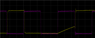
  • I don't have your example, but something similar that maybe can help you. You can see on scope picture one typical SBW cycle with 1 MHz CLK. Data is yellow.

    After master send 2 bits (one high and one low) to target device and after CLK reached high state, master release data line for target device respond. RESET (data) is pulled high and there is rising slope. after CLK reached low state, target device change direction on data line and respond with bit high. After CLK reach high state target device change direction on data line again.

    In your case, at last clock you can leave clock high, and change both (clk and data) direction to input at the same moment. Clock (TEST pin) is pulled low and clock should go to low state with falling slope. With low CLK state target device should send respond bit. There must be longer delay than default is, and (if it is working) SBW interface will be slower. After master read data from target it should put new bit on data line, and switch both (clk and data) direction to out. In this moment there will be some short circuit (in case of different master / target data signal), but this should be absorbed by resistor on data line.

    Once again, I am not sure that this will work, but I am sure that during debugging you must watching both (clk and data) signals with scope (not with logic analyzer).

  • Thanks! I will give it a try.

    If I do short circuit the signals (TDOI from SN74AVC4T774RSV to TDO of the MSP430F5438A) can I damage the chips? The schematic does not show any resistor on those lines.

  • I guess that before changing direction (from in to out), putting on data line value on master side that was read from target device,  is safe enough.

  • That method does not work on our unit, thanks for the suggestion. Two final questions, once again thank you for all your assistance:

    1 - If I have TDO= connected to a SN74AVC4T774RSV output pin that = 0 (or vice versa) can I damage the device or impact SBW operation?

         MSP430 TDO  high --------><----------- low   SN74AVC4T774RSV

    2 - Do you see any way to program the MSP430F5438A using only writes from the host?

    Thank you for your time.

  • SBW cycle is defined as 2 bits out and one in (from host side) and this can't be changed. It can be aligned for ignoring last in bit, but not sure if shrinking last (low) clock cycle to minimum period should help to not have short on data line. I never analyzed this, so don't know.

    If UART (or any other) connection with master exists, than can be used factory BSL (or customized) version. There is no problem to enter in BSL mode by one way TEST / RESET sequence from master side. Factory BSL is not, but customized version can work with only one way write from host.

**Attention** This is a public forum