Part Number: MSP430FR4133
Other Parts Discussed in Thread: MSP430G2553
Im trying to map code from an existing library I found so that I can drive a ws2812b LED strip. I found the library here https://github.com/mjmeli/MSP430-NeoPixel-WS2812-Library. Ive made an attempt at mapping it for my specific part but the code still does not seem to work. There are 3 small sections that I need to change for my specific part and here are my attempts. The 3 blocks of code include the original code as well as my equivalent code. I need help with identifying a problem or some tips on how to map code from one MSP to another as I have no experience with doing so.
The first section is needed to configure the UCB0SIMO as the SPI Output
// ORIGINAL
#define OUTPUT_PIN  (0x80)  // Set to whatever UCB0SIMO is on your processor (Px.7 here)

P1SEL |= OUTPUT_PIN;    // configure output pin as SPI output
P1SEL2 |= OUTPUT_PIN;

//My equivalent code

P5SEL0 |= BIT2;    // configure output pin as SPI output
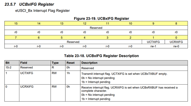
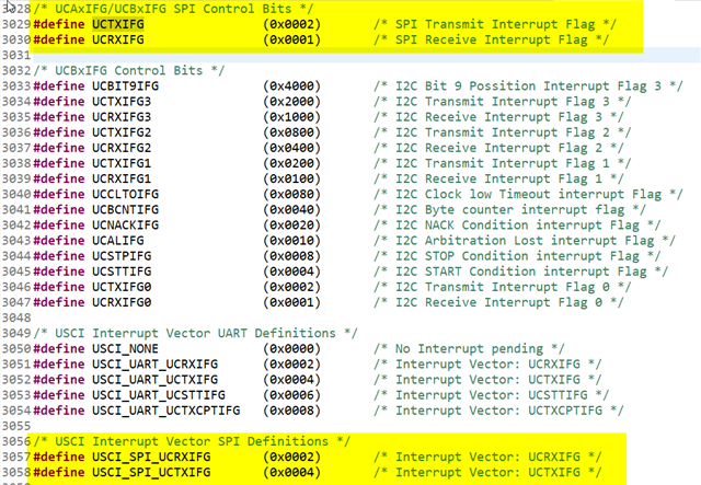
The second is checking the UCB interrupt flags. This is where I think the problem may be coming from? On the datasheet for my part this is in the data sheet: UCB0RXIFG, UCB0TXIFG (SPI mode) but when I use them I get an undefined error.
// Original Code

while (!(IFG2 & UCB0TXIFG))
;    // wait to transmit

// My equivalent code
while (!(SFRIFG1 & UCTXIFG))
;    // wait to transmit
And the 3rd section is initialising a 16 MHz clock
//Original Code

    if (CALBC1_16MHZ==0xFF)    // If calibration constant erased
    {
        while(1);              // do not load, trap CPU!!
    }

    // configure clock to 16 MHz
    BCSCTL1 = CALBC1_16MHZ;    // DCO = 16 MHz
    DCOCTL = CALDCO_16MHZ;


// My equivalent code

void initClockTo16MHz()
{
    // Configure one FRAM waitstate as required by the device datasheet for MCLK
    // operation beyond 8MHz _before_ configuring the clock system.
    FRCTL0 = FRCTLPW | NWAITS_1;

    __bis_SR_register(SCG0);    // disable FLL
    CSCTL3 |= SELREF__REFOCLK;  // Set REFO as FLL reference source
    CSCTL0 = 0;                 // clear DCO and MOD registers
    CSCTL1 &= ~(DCORSEL_7);     // Clear DCO frequency select bits first
    CSCTL1 |= DCORSEL_5;        // Set DCO = 16MHz
    CSCTL2 = FLLD_0 + 487;      // set to fDCOCLKDIV = (FLLN + 1)*(fFLLREFCLK/n)
                                //                   = (487 + 1)*(32.768 kHz/1)
                                //                   = 16 MHz

    __delay_cycles(3);
    __bic_SR_register(SCG0);                        // enable FLL
    while(CSCTL7 & (FLLUNLOCK0 | FLLUNLOCK1));      // FLL locked

    CSCTL4 = SELMS__DCOCLKDIV | SELA__REFOCLK;
}