Hi,
I’m doing some tests with FLL locked to external low power crystal which is 32.768Khz.
My aim is to obtain proper 8Mhz MCLK (as much as possible jitter-free)
With disabled modulation:
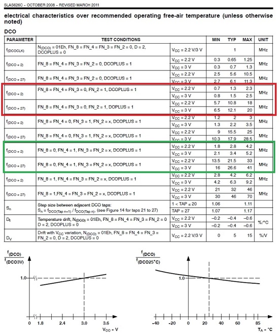
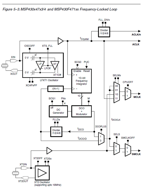
SCFI0 = FN_2 | FLLD0; // FN_2 (1.3 to 12.1 MHz); D = 2
FLL_CTL0 = DCOPLUS | XCAP0PF; // DCO+ set, fDCOCLK = D x (N + 1) x fACLK, 0pF
SCFQCTL = 121 | 128; // FMCLK = 2*(121+1)*32768 = 7.995392 MHz
Min Freq : 7.86Mhz
Max Freq : 8.73Mhz
Mean Freq : 8.22Mhz
With enabled modulation:
SCFI0 = FN_2 | FLLD0; // FN_2 (1.3 to 12.1 MHz); D = 2
FLL_CTL0 = DCOPLUS | XCAP0PF; // DCO+ set, fDCOCLK = D x (N + 1) x fACLK, 0pF
SCFQCTL = 121; // FMCLK = 2*(121+1)*32768 = 7.995392 MHz
Min Freq : 7.896Mhz
Max Freq : 8.669Mhz
Mean Freq : 8.00Mhz
Std Dev : ~250Khz
In my tests, I saw that higher frequencies have less jitter for example 16Mhz, but how that can be possible? What are the relations between FN_x, D, SCFQCTL parameters and jitter?
Thanks