Other Parts Discussed in Thread: CAPTIVATE-FR2676
Hi,
My customer is designing the board and referring "Capacitive Touch Design Flow for MSP430 MCUs with CapTIvate Technology" SLAA842B.
In section "Step 4b.5: Sensor Traces", it says;
Q1) "half of the panel thickness" means "half of PCB thickness"?
For example, if PCB thickness is 1.6mm, GND needs to be separated >0.8mm from TX or RX?
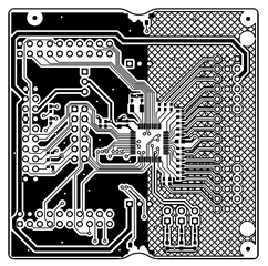
According to the customer, TI reference board does not meet it.
Q2) What is the purpose to keep such distance between GND and Tx (or Rx)?
Q3) Are these guidelines targeted for double sided boards or single sided boards or both?
Thanks and regards,
Koichiro Tashiro