This thread has been locked.

If you have a related question, please click the "Ask a related question" button in the top right corner. The newly created question will be automatically linked to this question.

MSP430I2041: PGA performance

Part Number: MSP430I2041
Other Parts Discussed in Thread: ADS1220, , ADS1299

Hi, 

Input common mode : 

o In the datasheet §8.7.7.4 : Common mode input voltage range [AVSS-1 ; Vcc] : I'm surprised that this doesn't depend on the PGA gain (like the ADS1220), is it really independent ?
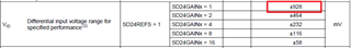
o In datasheet §8.7.7.6: "SD24GAINx = 1, Common-mode input signal:?? VID = 928 mV, fIN = 50 Hz":
->  What is the value of the common-mode voltage that gives the values of this field?
->  Do you have a curve of the CMRR as a function of the frequency of the common-mode voltage? (I'm particularly interested in the case where the PGA is 1 [V/V]).

On input impedance:

-> do you have more information? In particular, how do you distinguish part/part variability @ 25°C from thermal sensitivity?

Regards,

Geoffrey

  • HI,

    1. Common mode input voltage range [AVSS-1 ; Vcc]. It is independent from the PGA settings. If you set an inappropriate gain setting, you will get a distorted signal.

    2. What is the value of the common-mode voltage that gives the values of this field? The test condition is external reference voltage is 1.2 V., over operating free-air temperature range (unless otherwise noted)

    3.I do not think we have the CMRR curve. What we have are already in the datasheet. 

    Best regards,

    Cash Hao

  • Hi,

    Goeffrey kindly open this subject for me.

    First, thank you for your attention and answers.

    Context:

    For a new project, we need to design a “tiny” sensor acquisition chain (very small area of PCB available for this function).

    This chain shall integrates all functions needed to convert signal from sensor outputs to a digital value proportional to the physical quantity to measure.

    The sensor outputs is a couple of voltages ( called “A” and “B”) with following main specifications:

    • Analog
    • Differential
    • Frequency < 10 Hz
    • The physical quantity to measure is included in the ratio between these voltages
    • Voltage range ~ 1Vpp
    • Source output impedance : [1; 10] kOhms

    This function will be submitted to important thermal variations ( first approximation: [-40;+100]°C).

    An initial calibration is considered. If applied, this calibration, would be applied on each chain (sensor; acquisition chain), one time (just after board assembly), at +25°C  (no temperature compensation embedded)

    As this chain can be used for human safety function, we have to prove function performances both by tests AND by theoretical analysis. That the reasons why we need some details about measurement uncertainty contributors and their variations versus temperature and time.


    Current step of design:

    In a first approach, MSP430I2041 seems a good candidate as it is “small”, no not a lot of external peripherals and it integrates (ADC sigma delta+ PGA).  

    But, we need some additional data, compared to datasheet, to establish our proof of design and performances.

    Questions about SD24 of MSP430I2041 :

    • With hypothesis of one shared SD24 channel used to acquire sequentially each sensor outputs voltages :
      • Inside ONE SD24 channel, between inputs differential pairs, do you have data about mismatch in terms of:
        • Input impedances (differential and single ended) ?
        • Offset error ?
        • Gain error ?
        • Integral non linearity ?
        • Input current leakage ?


    • With hypothesis of one SD24 used by each sensor output voltage (simultaneous sampling):
      • Do you have data about input impedances (differential and single ended) temperature coefficient?

    Global question:

    Do you have other device references to propose, which seems best fitted for our context?


    Best regards,

    Emilien


  • 1. For your signal, please pay attention to the input voltage range

    2. Here is the input impendance you can find in the datasheet:

    3. Here is the offset error with internal reference, for external reference, please refer to the datasheet:

    4. It is not fair to ask GAIN error and INL and DNL for SD ADC. That is for SAR ADC.  Because INL is obtained from a plot of digital output code as a function of its analog input voltage level while the sigma-delta ADC has 1bit (2 levels) digital output bitstream. However, the OPA have the gain error:

    5. Sorry, I can't find this parameter. Can you tell me why you care about the leackage current.

  • Hi, thank you for your answer.

    I think that there is a little misunderstanding, as i am searching  data about:

    Inside ONE SD24 channel, between inputs differential pairs, do you have data about mismatch in terms of.."

    Best regards,

    Emilien

  • Can you give an example of such data?

  • Hi,

    For example (arbitrary) on ADS1299 , there are "Gain match between channels" specification.

  • Hi,

    For example (arbitrary) on ADS1299 , there are "Gain match between channels" specification.

  • Does this can meet your requirement?

  • No, as it is for one channel, not channel to channel mismatch.

  • Get your point, sorry, we don't have this parameter. See from the datasheet, the max mismatch, should be lower than 4%. If you want to reach higher accuarcy, I would suggest you do calibration.

**Attention** This is a public forum