Other Parts Discussed in Thread: MSP430FR5989
Hi,
I am trying to reproduce the error described in errata DMA7 of MSP430FR5989 microcontroller, which states that a if a DMA request starts executing during the time when a module register containing an interrupt flags is accessed with a read-modify-write instruction, a newly arriving interrupt from the same module can get lost.
What I have done so far is the following:
__root const UCHAR DmaSrcData[] = {
	0x02, 0x00
};
void main( void )
{
	InitializeHardware(); // initialize ports, clocks, pmm, etc.

	// -------------- INIT TA1 ----------------------

	TA1CTL = TASSEL__ACLK
	         | ID__1
	         | MC__UP
	         | TACLR;

	TA1CCTL0 = !CAP
		       | OUTMOD_0
		       | !CCIE;

	TA1EX0 = TAIDEX_0;	/* divider /1 */

	// -------------- END INIT TA1 -------------------


	// -------------- INIT TB0 -----------------------
	TB0CTL = TBSSEL__ACLK
	         | ID__1
	         | MC__CONTINUOUS
	         | TBCLGRP_0
	         | CNTL_0
	         | TBCLR;

	TB0CCTL0 = !CAP
	           | OUTMOD_0
	           | CLLD_0
	           | !CCIE;

	TB0EX0 = TBIDEX_0;

	// -------------- END INIT TB0 -------------------


	// -------------- INIT DMA -----------------------
	// DMA is triggered by TA1CCR0 every 250ms.
	// Source data has two values (0x02 and 0x00) used to alternate the destination port output value (P4.1)

	DMA1CTL_bit.DMAEN = false;

	DMACTL4_bit.DMARMWDIS = true;

	DMACTL0 = ( DMACTL0 & ~DMA1TSEL_31 )
	          | DMA1TSEL__TA1CCR0;

	DMA1CTL |= DMADT2							// Repeated single transfer
	           |  !DMADSTINCR0 | !DMADSTINCR1	// Destination address is not incremented
	           |  DMASRCINCR0 | DMASRCINCR1		// Source address is incremented
	           |  DMASRCBYTE
	           |  DMADSTBYTE
	           |  !DMALEVEL
	           |  !DMAIFG
	           |  !DMAIE
	           |  !DMAABORT
	           |  !DMAREQ;

	DMA1SA = ( void * )&DmaSrcData[0];
	DMA1DA = ( void * )&P4OUT;
	DMA1SZ = 2;

	// -------------- END INIT DMA -----------------------


	TA1CCTL0_bit.CCIFG = false;

	TB0CCR0 = TB0R + 2;
	TB0CCTL0_bit.CCIFG = false;
	while ( !TB0CCTL0_bit.CCIFG ){
	}

	// DMA trigger timer and TB0.0 synchronization
	TA0CTL |= TACLR;	// clears DMA timer counter
	TB0CCR0 += 8192 - 1; // 8192 ticks = 250ms. A tick is sutracted to start clearing the TB0CCTL0 30us before the DMA request
	TB0CCTL0_bit.CCIFG = false;

	// DMA is triggered every 250ms
	TA1CCR0 = 8192; // 8192 ticks = 250ms
	DMA1CTL_bit.DMAEN = true;	// starts DMA

	for (;;) {
		while ( !TB0CCTL0_bit.CCIFG ){
		}
		TB0CCR0 += 8192 + 1;
		P3OUT = 0x80;	// trace P3.7

		// Continuously clears the TB0CCTL0 interruption flag from 30 us before the dma trigger to about 30us after.
		// The idea of this is to perform a read-modify-write operation on a register containing
		// an interruption flag at the same moment that the DMA is triggered.
		TB0CCTL0_bit.CCIFG = false; TB0CCTL0_bit.CCIFG = false; TB0CCTL0_bit.CCIFG = false; TB0CCTL0_bit.CCIFG = false;
		TB0CCTL0_bit.CCIFG = false; TB0CCTL0_bit.CCIFG = false; TB0CCTL0_bit.CCIFG = false; TB0CCTL0_bit.CCIFG = false;
		TB0CCTL0_bit.CCIFG = false; TB0CCTL0_bit.CCIFG = false; TB0CCTL0_bit.CCIFG = false; TB0CCTL0_bit.CCIFG = false;
		TB0CCTL0_bit.CCIFG = false; TB0CCTL0_bit.CCIFG = false; TB0CCTL0_bit.CCIFG = false; TB0CCTL0_bit.CCIFG = false;
		TB0CCTL0_bit.CCIFG = false; TB0CCTL0_bit.CCIFG = false; TB0CCTL0_bit.CCIFG = false; TB0CCTL0_bit.CCIFG = false;
		TB0CCTL0_bit.CCIFG = false; TB0CCTL0_bit.CCIFG = false; TB0CCTL0_bit.CCIFG = false; TB0CCTL0_bit.CCIFG = false;
		TB0CCTL0_bit.CCIFG = false; TB0CCTL0_bit.CCIFG = false; TB0CCTL0_bit.CCIFG = false; TB0CCTL0_bit.CCIFG = false;
		TB0CCTL0_bit.CCIFG = false; TB0CCTL0_bit.CCIFG = false; TB0CCTL0_bit.CCIFG = false; TB0CCTL0_bit.CCIFG = false;
		TB0CCTL0_bit.CCIFG = false; TB0CCTL0_bit.CCIFG = false; TB0CCTL0_bit.CCIFG = false; TB0CCTL0_bit.CCIFG = false;
		TB0CCTL0_bit.CCIFG = false; TB0CCTL0_bit.CCIFG = false; TB0CCTL0_bit.CCIFG = false; TB0CCTL0_bit.CCIFG = false;
		TB0CCTL0_bit.CCIFG = false; TB0CCTL0_bit.CCIFG = false; TB0CCTL0_bit.CCIFG = false; TB0CCTL0_bit.CCIFG = false;
		TB0CCTL0_bit.CCIFG = false; TB0CCTL0_bit.CCIFG = false; TB0CCTL0_bit.CCIFG = false; TB0CCTL0_bit.CCIFG = false;
		TB0CCTL0_bit.CCIFG = false; TB0CCTL0_bit.CCIFG = false; TB0CCTL0_bit.CCIFG = false; TB0CCTL0_bit.CCIFG = false;
		TB0CCTL0_bit.CCIFG = false; TB0CCTL0_bit.CCIFG = false; TB0CCTL0_bit.CCIFG = false; TB0CCTL0_bit.CCIFG = false;
		TB0CCTL0_bit.CCIFG = false; TB0CCTL0_bit.CCIFG = false; TB0CCTL0_bit.CCIFG = false; TB0CCTL0_bit.CCIFG = false;
		P3OUT = 0x00;	// trace P3.7
	}
}
The idea of this test is to trigger a DMA every 250ms (see Image1) and continuously perform read-modify-write operations (in this case, clear the TB0CCTL0 interrupt flag) from 30us before the DMA trigger until about 30us after the trigger to make sure there is a DMA request at the same time that the register is accessed. A trace is set before starting read-modify-write operations and cleared at the end of this process (see images 1 and 2). If, at any time, the trace period is about 2 seconds instead of 250ms, this would mean that an interrupt flag has been missed.
In the following images, CH1 (orange) is the trace signal (P3.7) and CH2 (blue) is the DMA destination port (P4.1).
Image 1:
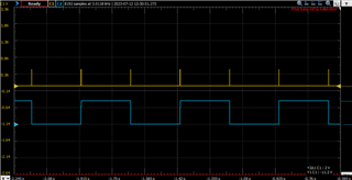
Image 2:
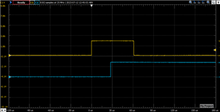
Read-modify-write operations are started 30us before the DMA trigger and stopped 30us after it.
I've left the code running for about 1 day now with no luck, which makes me think I might not be meeting the conditions of the errata.
Is this test correct? If not, what else could I try to replicate the errata?
Thanks.