This thread has been locked.

If you have a related question, please click the "Ask a related question" button in the top right corner. The newly created question will be automatically linked to this question.

Driving Boost Converter MOSFET's with MSP430G2452

Other Parts Discussed in Thread: MSP430G2452

Hello,

I am trying to designing a boost converter to run off a Li-ion battery. My problem is the driving of the MOSFET's in the converter. I want to use the MSP430 series microcontroller (specifically MSP430G2452). In some related forum posts users recommended that a gate driver be used i.e.

http://e2e.ti.com/support/microcontrollers/stellaris_arm_cortex-m3_microcontroller/f/471/p/54562/423769.aspx#423769

I have tried to understand the http://focus.ti.com/lit/ml/slup169/slup169.pdf document "Design And Application Guide For High Speed MOSFET Gate Drive Circuits", but i am just becoming confused with what circuit to use to drive my MOSFET's.

Below is my circuit with the MOSFET's i intend to use:

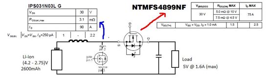
They are both NMOS and i have tried to select low Vgs(th) so i can drive straight from the micro.

I was just wondering if anyone could recommend a MOSFET driver that would suit my application?

Or advice on the type of gate driver circuits that would be best?

I realise i can drive the parallel MOSFET straight from the controller with an appropriate R(gate) (pg.10/11 of slup169.pdf) but still am open to direction. :)

Also am switching at 40kHz

Thanks

Michael Dalton

  • The low Vgs MOSFETs usually have a high gate capacitance (that's what you pay for the low voltage).
    The current driving capacity of the MSP ports is limited. So on higher switching frequencies, the high charge needed to drive the gate might become a problem. A gate driver will greatly increase this peak current and therefore decrease the switching time, also greatly decreasing the thermal losses during switching.

    In our laser project, we were controlling a 70A low Vgs MOSFET by an OpAmp with 60mA driving capability (far more than the MSP) Yet we were unable to get past ~30kHz. And on 30kHz it was a rather sinusodial signal and no square on/off. When adding another transistor stage behind the OpAmp, things improved significantly.

    Michael Dalton said:
    I realise i can drive the parallel MOSFET straight from the controller with an appropriate R(gate)

    If you mean a series resistor with R(gate), then this would limit the frequency even further, by slowing down the current flow.

    Let's assume the MSP drives 10mA. On 40kHz switching frequency, this are 0.01A * 0.000025s = 250nAs. = 250nC charge. So what is the gate capacitance? In our case, it was as high as ~5nF. That means (not counting the dynamic response of the MSP ports on high currents, which makes things worse), that the rise time on the gate is 50V per switching cycle. With Vgson at least 1V, this means that the transistor will be 2% of a cycle in transition to on and 2% in transition to off for each required Volt on the gate. In reality it will be even worse. During this time, 100% energy is wasted on the transistor, beyond the (I2*RDSon). A separate gate driver which is optimized for short burts of charging/decharging teh gate, significantyl reduces this thime and significantly reduces losses as well as transistor heating.

  • Ok,

    So a separate gate driver is needed to allow the device to switch normally at higher frequencies.

    If i were to use a PMOS for the high side switch, i could use the same gate driver for the low side NMOS, but can you please clarify this for me?

    Slup169.pdf it says on page 18

    "the output of the PWM controller has to be inverted and referenced to the positive input rail"

    Does this mean that the PMOS is "off" when i have a logic HIGH (3.7V for example) on the gate and "on" when i have logic LOW (0v or GND)??

    Cheers

    Michael Dalton

  • Michael Dalton said:
    Does this mean that the PMOS is "off" when i have a logic HIGH (3.7V for example) on the gate

    Yes.

    PMOS requires a gate voltage lower than its source while NMOS requires a gate voltage higher than its drain. (with some threshold). When a PMOS is on, its drain voltage rises, while on an NMOS, the source voltage drops, based on the current and its RDSon. So in PMOS datasheets, you'll see a gate-source voltage threshold and VGS diagrams while on NMOS it is VGD that controls the state.

    It's like PNP and NPN transistors.

  • Sooo Also,

    Looking at datasheets, if i only have from 3.7V down to 0V to work with i have to pick a PMOSFET component with a Vth higher than 0??

    Some of the PFET's are saying to Vth min = -1. Would i be unable to drive this on with 0V?


    Sorry for the silly question,


    Regards


    Michael Dalton

  • Michael Dalton said:
    Some of the PFET's are saying to Vth min = -1. Would i be unable to drive this on with 0V?

    No. I tmeans that Vg needs to be at least 1V below Vs. (if Source is on VCC, then you need Vg < Vcc-1 before anythign happens). 0V is Vg-VCC and definitely enough. However, the more below the source the gate is, the lower the RDSon. (up to a limit).
    The resulting drain voltage might even be above the gate voltage once the FET is driving.

    if you have a PMOS with source tied to 3V and drain to a resistor to GND, then you will need to go below 2V with the gate before a current flows through the resistor. And when the gate is on 0V, almost full 3V will be on the resistor (so the gate voltage is well below the drain voltage).


    However, if you use a PMOS between the load and GND (on the low-side), then putting the gate to GND (or any fixed voltage) will result in sort of a self-regulating current-sink :)
    I used NMOS transistors as constant current sources by putting them top of the load, their gate tied to their source. (same applicaiton, just mirrored)

**Attention** This is a public forum