This thread has been locked.

If you have a related question, please click the "Ask a related question" button in the top right corner. The newly created question will be automatically linked to this question.

MSP430F6777A: MSP430F6777A microcontroller High speed GPIO toggle

Part Number: MSP430F6777A

I am using MSP430F6777A microcontroller. SMCLK frequency is 25MHz. I want to toggle GPIO pin to drive assembly led. For this operation, I need to keep the GPIO pin high for 900ns and low for 300ns. Operations such as if control, for loop and && logic operator increase the toggle time. How can I make the toggle process faster without using a timer in pwm mode?

AN1001_IC Embedded Solutions of SMD LEDs (Ver 1.0).pdf

TOH=300ns
T0L=900ns
T1H=900ns
T1L=300ns

  • Hi Selim 

    I checked the waveform the high signal is alway T1H=900ns and low signal is alway T1L=300ns.

    May I know when TOH=300ns and T0L=900ns are needed?

    Thanks

  • Hi ,
    If you want to send logic 0. The signal should be sent like this. (TOH=300ns and T0L=900ns)

  • Have you looked into using a PWM timer? No CPU involvement at all.

  • Hi Selim 

    Please check if PWM timer is OK for your application as Keith comment.

    Thanks

  • Hi Xiaodong, Hi Keith

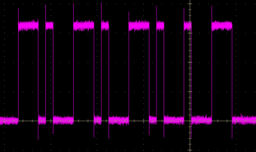
    If we are going to send the 10011001 logic information to the led driver, the signal we need to obtain should be as follows.

    We tried to change the duty value in each pwm interrupt to obtain the signal, but we did not get successful results.

  • I think the DMA should be able to do what you want. You could trigger on CCR0 to transfer a new CCRn comparison value. If the sequence is cyclic, you could put the entire sequence into an array and have it repeat (DMADT=4). The possible triggers -- i.e. choices for timers and CCRn -- are in data sheet (SLAS962A) Table 6-14.

    The DMA is fast (in any case faster than software) though not instantaneous. But with MCLK=25MHz your 40ns tick should be able to meet the update deadlines. [Timings: Ref User Guide (SLAU208Q) Table 11-3]

    [Edit: Added reference to DMA transfer times table.]

  • Hi Bruce,

    Thank you for your support. I tried the method you mentioned. But I could not change the duty value as I wanted.

    When I set the timer period value to 12us, I can accurately obtain data such as 10101001.

    But I cannot get the signal with the desired period value of 1.2us.

  • It does look (to my non-expert eye) like the DMA isn't keeping up, despite the User Guide.

    What is the CPU doing while this is happening? If it's not in LPM0 (Idle), is this something you can try? 

    [Ancient History: I once had a fight with the F2-series DMA. The symptom was an SPI overrun, as though the DMA wasn't keeping up -- regardless of the DMAONFETCH setting, which is supposed to allow the DMA to operate mid-instruction. This wasn't a spot where I could use LPM, so my workaround was to pad my polling loop with NOP-s (1xMCLK each) to give the DMA more opportunities, at which point  the symptom disappeared. I keep this in mind even now when I run the DMA close to its limits.]

  • Do you have a choice of which timer to use?

    I just succeeded with this (on an F5529) using TB0 with CLLD=2. Using the shadow register gives the DMA the entire period to update CCR2, which appears to be plenty of time. (It worked at SMCLK=25MHz, but 20MHz works better since 40 doesn't divide either 300 or 900.)

    There's still value in the DMA, since trying to update CCR2 with software in 24 clocks is rather tight.

    [Edit: Sorry, I just noticed the F6777A doesn't have a Timer B. I'm going to leave this here for the archaeologists.]

  • I've succeeded in generating the waveform you're looking for using this method. This was on an F5529, using TB0 with CLLD=0 (so it behaves the same as timerA). The timings (on my scope) are correct, within rounding error, at SMCLK=MCLK=25MHz (better at 20MHz).

    I still have some fringe artifacts I haven't explained, so I can't quite say "solved", but the fact that it Can succeed suggests that maybe there's something in your implementation (or particular to your device) causing the trouble you're seeing. 

  • Hi Bruce,

    Have you tried using TimerA? Can you share the code made with TimerB for reference?

  • Here's what I'm working with. It uses TA0 on an F5529. The second half of the code (clock setup) is pretty much pasted from a TI example.

    //
    //  Generate bit encoding with a timer.
    //  No warranty, no support. I may not even exist.
    //
    #include <msp430.h> 
    #include <stdint.h>
    #define HZ      20000000UL      // MCLK=SMCLK=20MHz
    //  Long and Short pulses, measured in timer (SMCLK) ticks. For 20MHz:
    #define SHORT   6               // 6*50ns  = 300ns
    #define LONG    (3*SHORT)       // 3*300ns = 900ns
    #define PERIOD  (LONG+SHORT)
    #define USE_LPM     0
    uint16_t bits[] = {LONG, SHORT, LONG, SHORT, LONG, SHORT, SHORT, LONG}; // 10101001
    //uint16_t bits[] = {LONG, LONG , SHORT, SHORT, LONG, SHORT, LONG, LONG}; // 11001011
    //uint16_t bits[] = {SHORT, LONG , SHORT, SHORT, LONG, SHORT, LONG, LONG}; // 01001011
    #define NBITS   (sizeof(bits)/sizeof(bits[0]))
    extern void setDCOtoHz(void);
    
    int main(void)
    {
    	WDTCTL = WDTPW | WDTHOLD;	// stop watchdog timer
    	
    	P1OUT &= ~BIT0;             // There's always an LED at P1.0,
    	P1DIR |=  BIT0;             //   right?
    #if HZ > 1000000UL              // Something other than post-reset speed
    	setDCOtoHz();
    #endif // HZ
    	P1DIR |= BIT3;              // P1.3 as TA0.2
    	P1SEL |= BIT3;              //  per SLAS590P Table 9-46
    
    	DMACTL0 = DMA0TSEL_1;       // TA0CCR0 per SLAS590P Table 9-10
    	__data20_write_long((uintptr_t) &DMA0SA, (uintptr_t)&bits[0]);
        __data20_write_long((uintptr_t) &DMA0DA, (uintptr_t)&TA0CCR2);
        DMA0SZ = NBITS;
        DMA0CTL = DMADT_0 | DMADSTINCR_0 | DMASRCINCR_3 | (0*DMADSTBYTE) | (0*DMASRCBYTE)
                | (0*DMALEVEL) | (0*DMAEN) | (USE_LPM*DMAIE);
    
        TA0CCR0 = PERIOD-1;
    	TA0CTL = TASSEL_2 | ID_0 | 0*MC__UP | TACLR;    // SMCLK/1, Up (soon)
    	__enable_interrupt();
    
    	while(1)
    	{
    	    P1OUT ^= BIT0;
            TA0CTL &= ~MC_3;         // Stop timer
            TA0CCTL0 &= ~CCIFG;      // Clear stale for DMA trigger edge
            TA0CCR2 = SHORT;         // Avoid early EQU2 (first-time-ever)
    	    TA0CCTL2 = OUTMOD_7;     // High pulse at the beginning
    	    DMA0CTL |= DMAEN;
    	    TA0CTL |= MC__UP|TACLR;  // Start timer
    #if USE_LPM
            LPM0;
    #else
            while (DMA0CTL & DMAEN)/*EMPTY*/;
    #endif
            TA0CCTL2 = OUTMOD_5;    // For last cycle just clear and leave it
    	    __delay_cycles(HZ/2);   // Pause to read the scope
    	}
    	/*NOTREACHED*/
    	return 0;
    }
    
    #if USE_LPM
    #pragma vector=DMA_VECTOR
    __interrupt void
    dma_ISR(void)
    {
        DMA0CTL &= ~DMAIFG;
        LPM0_EXIT;
        return;
    }
    #endif // USE_LPM
    
    //  Lifted from TI Example MSP430F55xx_UCS_10.c:
    void SetVcoreUp (unsigned int level)
    {
      // Open PMM registers for write
      PMMCTL0_H = PMMPW_H;
      // Set SVS/SVM high side new level
      SVSMHCTL = SVSHE + SVSHRVL0 * level + SVMHE + SVSMHRRL0 * level;
      // Set SVM low side to new level
      SVSMLCTL = SVSLE + SVMLE + SVSMLRRL0 * level;
      // Wait till SVM is settled
      while ((PMMIFG & SVSMLDLYIFG) == 0);
      // Clear already set flags
      PMMIFG &= ~(SVMLVLRIFG + SVMLIFG);
      // Set VCore to new level
      PMMCTL0_L = PMMCOREV0 * level;
      // Wait till new level reached
      if ((PMMIFG & SVMLIFG))
        while ((PMMIFG & SVMLVLRIFG) == 0);
      // Set SVS/SVM low side to new level
      SVSMLCTL = SVSLE + SVSLRVL0 * level + SVMLE + SVSMLRRL0 * level;
      // Lock PMM registers for write access
      PMMCTL0_H = 0x00;
    }
    //  Set the DCO to whatever HZ is (within DCORSEL=7)
    void
    setDCOtoHz(void)
    {
        // Increase Vcore setting to level3 to support fsystem=25MHz
        // NOTE: Change core voltage one level at a time..
        SetVcoreUp (0x01);
        SetVcoreUp (0x02);
        SetVcoreUp (0x03);
    
        UCSCTL3 = SELREF_2;                       // Set DCO FLL reference = REFO
        UCSCTL4 |= SELA_2;                        // Set ACLK = REFO
    
        __bis_SR_register(SCG0);                  // Disable the FLL control loop
        UCSCTL0 = 0x0000;                         // Set lowest possible DCOx, MODx
        UCSCTL1 = DCORSEL_7;                      // Select DCO range 50MHz operation
        UCSCTL2 = FLLD_0 + (HZ/32768)-1; //762;   // Set DCO Multiplier for 25MHz
                                                  // (N + 1) * FLLRef = Fdco
                                                  // (762 + 1) * 32768 = 25MHz
                                                  // Set FLL Div = fDCOCLK/2
        __bic_SR_register(SCG0);                  // Enable the FLL control loop
    
        // Worst-case settling time for the DCO when the DCO range bits have been
        // changed is n x 32 x 32 x f_MCLK / f_FLL_reference. See UCS chapter in 5xx
        // UG for optimization.
        // 32 x 32 x 25 MHz / 32,768 Hz ~ 780k MCLK cycles for DCO to settle
        __delay_cycles(782000);
    
        // Loop until XT1,XT2 & DCO stabilizes - In this case only DCO has to stabilize
        do
        {
          UCSCTL7 &= ~(XT2OFFG + XT1LFOFFG + DCOFFG);
                                                  // Clear XT2,XT1,DCO fault flags
          SFRIFG1 &= ~OFIFG;                      // Clear fault flags
        }while (SFRIFG1&OFIFG);                   // Test oscillator fault flag
    }
    

  • Hi Bruce

    I can get the correct signals when I configured it for my microcontroller. Thank you for your support.

**Attention** This is a public forum