This thread has been locked.

If you have a related question, please click the "Ask a related question" button in the top right corner. The newly created question will be automatically linked to this question.

MSP430F5522: BQ32002 RTC read failed on MSP430F5522

Part Number: MSP430F5522
Other Parts Discussed in Thread: BQ32002

Tool/software:

Hi Team,

Good wishes to you!  I'm working with the MSP430F5522 on my custom board. I need to read RTC time from the microcontroller (using I2C) to check if the time data is working properly or not. I'm using an external RTC, BQ32002.

I have successfully written and read. but I have problems during reading/seting time.

Problem is, I set a time like 85, 88, 35, 1, 49, 18, 35; // 31/12/2023 23:58:55
But each time, I got wrong date data such as:

in debug mode, the read data is as "0x7A, 0x25, 0x77, 0x07, 0x3C, 0xFF".

it seems BQ32002 doesn't work at the normal state.

Here is my code (with silght change for BQ32002) from MSP5522 code library: https://dev.ti.com/tirex/explore/node?node=A__AKT9feld19D8QYxvBMQtww__msp430ware__IOGqZri__LATEST
MSP430F55xx_usci_i2c_standard_master.c 

//******************************************************************************
//   MSP430F552x Demo - USCI_B0, I2C Master multiple byte TX/RX
//
//   Description: I2C master communicates to I2C slave sending and receiving
//   3 different messages of different length. I2C master will enter LPM0 mode
//   while waiting for the messages to be sent/receiving using I2C interrupt.
//   ACLK = NA, MCLK = SMCLK = DCO 16MHz.
//
//                                     /|\ /|\
//                   MSP430F5529       4.7k |
//                 -----------------    |  4.7k
//            /|\ |             P3.1|---+---|-- I2C Clock (UCB0SCL)
//             |  |                 |       |
//             ---|RST          P3.0|-------+-- I2C Data (UCB0SDA)
//                |                 |
//                |                 |
//                |                 |
//                |                 |
//                |                 |
//                |                 |
//
//   Nima Eskandari
//   Texas Instruments Inc.
//   April 2017
//   Built with CCS V7.0
//******************************************************************************

#include <msp430.h> 
#include <stdint.h>
#include <stdbool.h>


//******************************************************************************
// Example Commands ************************************************************
//******************************************************************************

//#define SLAVE_ADDR  0x48
#define SLAVE_ADDR 0x68

/* CMD_TYPE_X_SLAVE are example commands the master sends to the slave.
 * The slave will send example SlaveTypeX buffers in response.
 *
 * CMD_TYPE_X_MASTER are example commands the master sends to the slave.
 * The slave will initialize itself to receive MasterTypeX example buffers.
 * */

#define CMD_TYPE_0_SLAVE      0
#define CMD_TYPE_1_SLAVE      1
#define CMD_TYPE_2_SLAVE      2

#define CMD_TYPE_0_MASTER      0
#define CMD_TYPE_1_MASTER      4
#define CMD_TYPE_2_MASTER      5

#define TYPE_0_LENGTH   7
#define TYPE_1_LENGTH   2
#define TYPE_2_LENGTH   6

#define MAX_BUFFER_SIZE     20

/* MasterTypeX are example buffers initialized in the master, they will be
 * sent by the master to the slave.
 * SlaveTypeX are example buffers initialized in the slave, they will be
 * sent by the slave to the master.
 * */

uint8_t MasterType2 [TYPE_2_LENGTH] = {'F', '4', '1', '9', '2', 'B'};
uint8_t MasterType1 [TYPE_1_LENGTH] = { 8, 9};
uint8_t MasterType0 [TYPE_0_LENGTH] = { 85, 88, 35, 1, 49, 18, 35}; // {28/04/2023 01:57:01 pm}


uint8_t SlaveType2 [TYPE_2_LENGTH] = {0};
uint8_t SlaveType1 [TYPE_1_LENGTH] = {0};
uint8_t SlaveType0 [TYPE_0_LENGTH] = {0};
uint8_t SlaveByte [1] = {0};


//******************************************************************************
// General I2C State Machine ***************************************************
//******************************************************************************

typedef enum I2C_ModeEnum{
    IDLE_MODE,
    NACK_MODE,
    TX_REG_ADDRESS_MODE,
    RX_REG_ADDRESS_MODE,
    TX_DATA_MODE,
    RX_DATA_MODE,
    SWITCH_TO_RX_MODE,
    SWITHC_TO_TX_MODE,
    TIMEOUT_MODE
} I2C_Mode;

/* Used to track the state of the software state machine*/
I2C_Mode MasterMode = IDLE_MODE;

/* The Register Address/Command to use*/
uint8_t TransmitRegAddr = 0;

/* ReceiveBuffer: Buffer used to receive data in the ISR
 * RXByteCtr: Number of bytes left to receive
 * ReceiveIndex: The index of the next byte to be received in ReceiveBuffer
 * TransmitBuffer: Buffer used to transmit data in the ISR
 * TXByteCtr: Number of bytes left to transfer
 * TransmitIndex: The index of the next byte to be transmitted in TransmitBuffer
 * */
uint8_t ReceiveBuffer[MAX_BUFFER_SIZE] = {0};
uint8_t RXByteCtr = 0;
uint8_t ReceiveIndex = 0;
uint8_t TransmitBuffer[MAX_BUFFER_SIZE] = {0};
uint8_t TXByteCtr = 0;
uint8_t TransmitIndex = 0;

/* I2C Write and Read Functions */

/* For slave device with dev_addr, writes the data specified in *reg_data
 *
 * dev_addr: The slave device address.
 *           Example: SLAVE_ADDR
 * reg_addr: The register or command to send to the slave.
 *           Example: CMD_TYPE_0_MASTER
 * *reg_data: The buffer to write
 *           Example: MasterType0
 * count: The length of *reg_data
 *           Example: TYPE_0_LENGTH
 *  */
I2C_Mode I2C_Master_WriteReg(uint8_t dev_addr, uint8_t reg_addr, uint8_t *reg_data, uint8_t count);

/* For slave device with dev_addr, read the data specified in slaves reg_addr.
 * The received data is available in ReceiveBuffer
 *
 * dev_addr: The slave device address.
 *           Example: SLAVE_ADDR
 * reg_addr: The register or command to send to the slave.
 *           Example: CMD_TYPE_0_SLAVE
 * count: The length of data to read
 *           Example: TYPE_0_LENGTH
 *  */
I2C_Mode I2C_Master_ReadReg(uint8_t dev_addr, uint8_t reg_addr, uint8_t count);
void CopyArray(uint8_t *source, uint8_t *dest, uint8_t count);

I2C_Mode I2C_Master_ReadReg(uint8_t dev_addr, uint8_t reg_addr, uint8_t count)
{
    /* Initialize state machine */
    MasterMode = TX_REG_ADDRESS_MODE;
    TransmitRegAddr = reg_addr;
    RXByteCtr = count;
    TXByteCtr = 0;
    ReceiveIndex = 0;
    TransmitIndex = 0;

    /* Initialize slave address and interrupts */
    UCB0I2CSA = dev_addr;
    UCB0IFG &= ~(UCTXIFG + UCRXIFG);       // Clear any pending interrupts
    UCB0IE &= ~UCRXIE;                       // Disable RX interrupt
    UCB0IE |= UCTXIE;                        // Enable TX interrupt

    UCB0CTL1 |= UCTR + UCTXSTT;             // I2C TX, start condition
    __bis_SR_register(LPM0_bits + GIE);              // Enter LPM0 w/ interrupts

    return MasterMode;

}


I2C_Mode I2C_Master_WriteReg(uint8_t dev_addr, uint8_t reg_addr, uint8_t *reg_data, uint8_t count)
{
    /* Initialize state machine */
    MasterMode = TX_REG_ADDRESS_MODE;
    TransmitRegAddr = reg_addr;

    //Copy register data to TransmitBuffer
    CopyArray(reg_data, TransmitBuffer, count);

    TXByteCtr = count;
    RXByteCtr = 0;
    ReceiveIndex = 0;
    TransmitIndex = 0;

    /* Initialize slave address and interrupts */
    UCB0I2CSA = dev_addr;
    UCB0IFG &= ~(UCTXIFG + UCRXIFG);       // Clear any pending interrupts
    UCB0IE &= ~UCRXIE;                       // Disable RX interrupt
    UCB0IE |= UCTXIE;                        // Enable TX interrupt

    UCB0CTL1 |= UCTR + UCTXSTT;             // I2C TX, start condition
    __bis_SR_register(LPM0_bits + GIE);              // Enter LPM0 w/ interrupts

    return MasterMode;
}

void CopyArray(uint8_t *source, uint8_t *dest, uint8_t count)
{
    uint8_t copyIndex = 0;
    for (copyIndex = 0; copyIndex < count; copyIndex++)
    {
        dest[copyIndex] = source[copyIndex];
    }
}

//******************************************************************************
// Device Initialization *******************************************************
//******************************************************************************

void initClockTo16MHz()
{
    UCSCTL3 |= SELREF_2;                      // Set DCO FLL reference = REFO
    UCSCTL4 |= SELA_2;                        // Set ACLK = REFO
    __bis_SR_register(SCG0);                  // Disable the FLL control loop
    UCSCTL0 = 0x0000;                         // Set lowest possible DCOx, MODx
    UCSCTL1 = DCORSEL_5;                      // Select DCO range 16MHz operation
    UCSCTL2 = FLLD_0 + 487;                   // Set DCO Multiplier for 16MHz
                                              // (N + 1) * FLLRef = Fdco
                                              // (487 + 1) * 32768 = 16MHz
                                              // Set FLL Div = fDCOCLK
    __bic_SR_register(SCG0);                  // Enable the FLL control loop

    // Worst-case settling time for the DCO when the DCO range bits have been
    // changed is n x 32 x 32 x f_MCLK / f_FLL_reference. See UCS chapter in 5xx
    // UG for optimization.
    // 32 x 32 x 16 MHz / 32,768 Hz = 500000 = MCLK cycles for DCO to settle
    __delay_cycles(500000);//
    // Loop until XT1,XT2 & DCO fault flag is cleared
    do
    {
        UCSCTL7 &= ~(XT2OFFG + XT1LFOFFG + DCOFFG); // Clear XT2,XT1,DCO fault flags
        SFRIFG1 &= ~OFIFG;                          // Clear fault flags
    }while (SFRIFG1&OFIFG);                         // Test oscillator fault flag
}

uint16_t setVCoreUp(uint8_t level){
    uint32_t PMMRIE_backup, SVSMHCTL_backup, SVSMLCTL_backup;

    //The code flow for increasing the Vcore has been altered to work around
    //the erratum FLASH37.
    //Please refer to the Errata sheet to know if a specific device is affected
    //DO NOT ALTER THIS FUNCTION

    //Open PMM registers for write access
    PMMCTL0_H = 0xA5;

    //Disable dedicated Interrupts
    //Backup all registers
    PMMRIE_backup = PMMRIE;
    PMMRIE &= ~(SVMHVLRPE | SVSHPE | SVMLVLRPE |
                SVSLPE | SVMHVLRIE | SVMHIE |
                SVSMHDLYIE | SVMLVLRIE | SVMLIE |
                SVSMLDLYIE
                );
    SVSMHCTL_backup = SVSMHCTL;
    SVSMLCTL_backup = SVSMLCTL;

    //Clear flags
    PMMIFG = 0;

    //Set SVM highside to new level and check if a VCore increase is possible
    SVSMHCTL = SVMHE | SVSHE | (SVSMHRRL0 * level);

    //Wait until SVM highside is settled
    while((PMMIFG & SVSMHDLYIFG) == 0)
    {
        ;
    }

    //Clear flag
    PMMIFG &= ~SVSMHDLYIFG;

    //Check if a VCore increase is possible
    if((PMMIFG & SVMHIFG) == SVMHIFG)
    {
        //-> Vcc is too low for a Vcore increase
        //recover the previous settings
        PMMIFG &= ~SVSMHDLYIFG;
        SVSMHCTL = SVSMHCTL_backup;

        //Wait until SVM highside is settled
        while((PMMIFG & SVSMHDLYIFG) == 0)
        {
            ;
        }

        //Clear all Flags
        PMMIFG &= ~(SVMHVLRIFG | SVMHIFG | SVSMHDLYIFG |
                     SVMLVLRIFG | SVMLIFG |
                     SVSMLDLYIFG
                     );

        //Restore PMM interrupt enable register
        PMMRIE = PMMRIE_backup;
        //Lock PMM registers for write access
        PMMCTL0_H = 0x00;
        //return: voltage not set
        return false;
    }

    //Set also SVS highside to new level
    //Vcc is high enough for a Vcore increase
    SVSMHCTL |= (SVSHRVL0 * level);

    //Wait until SVM highside is settled
    while((PMMIFG & SVSMHDLYIFG) == 0)
    {
        ;
    }

    //Clear flag
    PMMIFG &= ~SVSMHDLYIFG;

    //Set VCore to new level
    PMMCTL0_L = PMMCOREV0 * level;

    //Set SVM, SVS low side to new level
    SVSMLCTL = SVMLE | (SVSMLRRL0 * level) |
               SVSLE | (SVSLRVL0 * level);

    //Wait until SVM, SVS low side is settled
    while((PMMIFG & SVSMLDLYIFG) == 0)
    {
        ;
    }

    //Clear flag
    PMMIFG &= ~SVSMLDLYIFG;
    //SVS, SVM core and high side are now set to protect for the new core level

    //Restore Low side settings
    //Clear all other bits _except_ level settings
    SVSMLCTL &= (SVSLRVL0 + SVSLRVL1 + SVSMLRRL0 +
                 SVSMLRRL1 + SVSMLRRL2
                 );

    //Clear level settings in the backup register,keep all other bits
    SVSMLCTL_backup &=
        ~(SVSLRVL0 + SVSLRVL1 + SVSMLRRL0 + SVSMLRRL1 + SVSMLRRL2);

    //Restore low-side SVS monitor settings
    SVSMLCTL |= SVSMLCTL_backup;

    //Restore High side settings
    //Clear all other bits except level settings
    SVSMHCTL &= (SVSHRVL0 + SVSHRVL1 +
                 SVSMHRRL0 + SVSMHRRL1 +
                 SVSMHRRL2
                 );

    //Clear level settings in the backup register,keep all other bits
    SVSMHCTL_backup &=
        ~(SVSHRVL0 + SVSHRVL1 + SVSMHRRL0 + SVSMHRRL1 + SVSMHRRL2);

    //Restore backup
    SVSMHCTL |= SVSMHCTL_backup;

    //Wait until high side, low side settled
    while(((PMMIFG & SVSMLDLYIFG) == 0) &&
          ((PMMIFG & SVSMHDLYIFG) == 0))
    {
        ;
    }

    //Clear all Flags
    PMMIFG &= ~(SVMHVLRIFG | SVMHIFG | SVSMHDLYIFG |
                SVMLVLRIFG | SVMLIFG | SVSMLDLYIFG
                );

    //Restore PMM interrupt enable register
    PMMRIE = PMMRIE_backup;

    //Lock PMM registers for write access
    PMMCTL0_H = 0x00;

    return true;
}

bool increaseVCoreToLevel2()
{
    uint8_t level = 2;
    uint8_t actlevel;
    bool status = true;

    //Set Mask for Max. level
    level &= PMMCOREV_3;

    //Get actual VCore
    actlevel = PMMCTL0 & PMMCOREV_3;

    //step by step increase or decrease
    while((level != actlevel) && (status == true))
    {
        if(level > actlevel)
        {
            status = setVCoreUp(++actlevel);
        }
    }

    return (status);
}

void initGPIO()
{
    //LEDs
    P1OUT = 0x00;                             // P1 setup for LED & reset output
    P1DIR |= BIT0;

    P4DIR |= BIT7;
    P4OUT &= ~(BIT7);

    //I2C Pins
    P3SEL |= BIT0 + BIT1;                     // P3.0,1 option select

    P2OUT=0X00; 
    P2DIR=0XFF; 

    //#define Buzzer_OFF      
    P2OUT&=~0X80;
}

void initI2C()
{
    UCB0CTL1 |= UCSWRST;                      // Enable SW reset
    UCB0CTL0 = UCMST + UCMODE_3 + UCSYNC;     // I2C Master, synchronous mode
    UCB0CTL1 = UCSSEL_2 + UCSWRST;            // Use SMCLK, keep SW reset
    UCB0BR0 = 160;                            // fSCL = SMCLK/160 = ~100kHz
    UCB0BR1 = 0;
    UCB0I2CSA = SLAVE_ADDR;                   // Slave Address is 048h
    UCB0CTL1 &= ~UCSWRST;                     // Clear SW reset, resume operation
    UCB0IE |= UCNACKIE;
}

//******************************************************************************
// Main ************************************************************************
// Send and receive three messages containing the example commands *************
//******************************************************************************
#define BQ32K_SECONDS		0x00	/* Seconds register address */
#define BQ32K_SECONDS_MASK	0x7F	/* Mask over seconds value */
#define BQ32K_STOP		0x80	/* Oscillator Stop flat */

#define BQ32K_MINUTES		0x01	/* Minutes register address */
#define BQ32K_MINUTES_MASK	0x7F	/* Mask over minutes value */
#define BQ32K_OF		0x80	/* Oscillator Failure flag */

#define BQ32K_HOURS_MASK	0x3F	/* Mask over hours value */
#define BQ32K_CENT		0x40	/* Century flag */
#define BQ32K_CENT_EN		0x80	/* Century flag enable bit */

#define BQ32K_CALIBRATION	0x07	/* CAL_CFG1, calibration and control */
#define BQ32K_TCH2		0x08	/* Trickle charge enable */
#define BQ32K_CFG2		0x09	/* Trickle charger control */

int main(void) {

    WDTCTL = WDTPW | WDTHOLD;                 // Stop watchdog timer

    increaseVCoreToLevel2();
    initClockTo16MHz();
    initGPIO();
    initI2C();

#if 0
    I2C_Master_WriteReg(SLAVE_ADDR, CMD_TYPE_0_MASTER, MasterType0, TYPE_0_LENGTH);
    I2C_Master_WriteReg(SLAVE_ADDR, CMD_TYPE_1_MASTER, MasterType1, TYPE_1_LENGTH);
    I2C_Master_WriteReg(SLAVE_ADDR, CMD_TYPE_2_MASTER, MasterType2, TYPE_2_LENGTH);

    I2C_Master_ReadReg(SLAVE_ADDR, CMD_TYPE_0_SLAVE, TYPE_0_LENGTH);
    CopyArray(ReceiveBuffer, SlaveType0, TYPE_0_LENGTH);

    I2C_Master_ReadReg(SLAVE_ADDR, CMD_TYPE_1_SLAVE, TYPE_1_LENGTH);
    CopyArray(ReceiveBuffer, SlaveType1, TYPE_1_LENGTH);

    I2C_Master_ReadReg(SLAVE_ADDR, CMD_TYPE_2_SLAVE, TYPE_2_LENGTH);
    CopyArray(ReceiveBuffer, SlaveType2, TYPE_2_LENGTH);
#else
    {
        //int error;
        uint8_t reg;
        
        /* Check Oscillator Stop flag */
        I2C_Master_ReadReg(SLAVE_ADDR, BQ32K_SECONDS, 1);
        CopyArray(ReceiveBuffer, SlaveByte, 1);
        reg=SlaveByte[0];
    
        if (reg & BQ32K_STOP) {
            // Oscillator was halted. Restarting
            reg &= ~BQ32K_STOP;
            SlaveByte[0]=reg;
            I2C_Master_WriteReg(SLAVE_ADDR, BQ32K_SECONDS, SlaveByte, 1);
        }
    
        /* Check Oscillator Failure flag */
        I2C_Master_ReadReg(SLAVE_ADDR, BQ32K_MINUTES, 1);
        CopyArray(ReceiveBuffer, SlaveByte, 1);
        reg=SlaveByte[0];
        if (reg & BQ32K_OF)
        {
            //Oscillator Failure. Check RTC battery
            reg &= ~BQ32K_OF;
            SlaveByte[0]=reg;
            I2C_Master_WriteReg(SLAVE_ADDR, BQ32K_MINUTES, SlaveByte, 1);
        }


#if 0
        //This enables charging without the diode - we don't need no stinkin' diodes!
        SlaveByte[0]=0x45;
        I2C_Master_WriteReg(SLAVE_ADDR, BQ32K_CFG2, SlaveByte, 1);

        SlaveByte[0]=0x20;
        I2C_Master_WriteReg(SLAVE_ADDR, BQ32K_TCH2, SlaveByte, 1);
#endif
    }

    I2C_Master_WriteReg(SLAVE_ADDR, CMD_TYPE_0_MASTER, MasterType0, TYPE_0_LENGTH);
    // __delay_cycles(50000);
    // send(ReceiveBuffer,0);
    while(1)
    {
        {
           // int error;
            uint8_t reg;
            
            /* Check Oscillator Stop flag */
            I2C_Master_ReadReg(SLAVE_ADDR, BQ32K_SECONDS, 1);
            CopyArray(ReceiveBuffer, SlaveByte, 1);
            reg=SlaveByte[0];
        
            if (reg & BQ32K_STOP) {
                // Oscillator was halted. Restarting
                reg &= ~BQ32K_STOP;
                SlaveByte[0]=reg;
                I2C_Master_WriteReg(SLAVE_ADDR, BQ32K_SECONDS, SlaveByte, 1);
            }
        
            /* Check Oscillator Failure flag */
            I2C_Master_ReadReg(SLAVE_ADDR, BQ32K_MINUTES, 1);
            CopyArray(ReceiveBuffer, SlaveByte, 1);
            reg=SlaveByte[0];
            if (reg & BQ32K_OF)
            {
                //Oscillator Failure. Check RTC battery
                reg &= ~BQ32K_OF;
                SlaveByte[0]=reg;
                I2C_Master_WriteReg(SLAVE_ADDR, BQ32K_MINUTES, SlaveByte, 1);
            }
        }
    
        I2C_Master_ReadReg(SLAVE_ADDR, CMD_TYPE_0_SLAVE, TYPE_0_LENGTH);
        CopyArray(ReceiveBuffer, SlaveType0, TYPE_0_LENGTH);

        __delay_cycles(4000000);
        //send(ReceiveBuffer,0);
        //__delay_cycles(4000000);
        // send("FLDEC\n",0);
    }
#endif

    __bis_SR_register(LPM0_bits + GIE);
    return 0;
}

//******************************************************************************
// I2C Interrupt ***************************************************************
//******************************************************************************

#if defined(__TI_COMPILER_VERSION__) || defined(__IAR_SYSTEMS_ICC__)
#pragma vector=USCI_B0_VECTOR
__interrupt void USCI_B0_ISR(void)
#elif defined(__GNUC__)
void __attribute__ ((interrupt(USCI_B0_VECTOR))) USCI_B0_ISR (void)
#else
#error Compiler not supported!
#endif
{
  //Must read from UCB0RXBUF
  uint8_t rx_val = 0;

  switch(__even_in_range(UCB0IV,0xC))
  {
    case USCI_NONE:break;                             // Vector 0 - no interrupt
    case USCI_I2C_UCALIFG:break;                      // Interrupt Vector: I2C Mode: UCALIFG
    case USCI_I2C_UCNACKIFG:break;                    // Interrupt Vector: I2C Mode: UCNACKIFG
    case USCI_I2C_UCSTTIFG:break;                     // Interrupt Vector: I2C Mode: UCSTTIFG
    case USCI_I2C_UCSTPIFG:break;                     // Interrupt Vector: I2C Mode: UCSTPIFG
    case USCI_I2C_UCRXIFG:
        rx_val = UCB0RXBUF;
        if (RXByteCtr)
        {
          ReceiveBuffer[ReceiveIndex++] = rx_val;
          RXByteCtr--;
        }

        if (RXByteCtr == 1)
        {
          UCB0CTL1 |= UCTXSTP;
        }
        else if (RXByteCtr == 0)
        {
          UCB0IE &= ~UCRXIE;
          MasterMode = IDLE_MODE;
          __bic_SR_register_on_exit(CPUOFF);      // Exit LPM0
        }
        break;                      // Interrupt Vector: I2C Mode: UCRXIFG
    case USCI_I2C_UCTXIFG:
        switch (MasterMode)
        {
          case TX_REG_ADDRESS_MODE:
              UCB0TXBUF = TransmitRegAddr;
              if (RXByteCtr)
                  MasterMode = SWITCH_TO_RX_MODE;   // Need to start receiving now
              else
                  MasterMode = TX_DATA_MODE;        // Continue to transmission with the data in Transmit Buffer
              break;

          case SWITCH_TO_RX_MODE:
              UCB0IE |= UCRXIE;              // Enable RX interrupt
              UCB0IE &= ~UCTXIE;             // Disable TX interrupt
              UCB0CTL1 &= ~UCTR;            // Switch to receiver
              MasterMode = RX_DATA_MODE;    // State state is to receive data
              UCB0CTL1 |= UCTXSTT;          // Send repeated start
              if (RXByteCtr == 1)
              {
                  //Must send stop since this is the N-1 byte
                  while((UCB0CTL1 & UCTXSTT));
                  UCB0CTL1 |= UCTXSTP;      // Send stop condition
              }
              break;

          case TX_DATA_MODE:
              if (TXByteCtr)
              {
                  UCB0TXBUF = TransmitBuffer[TransmitIndex++];
                  TXByteCtr--;
              }
              else
              {
                  //Done with transmission
                  UCB0CTL1 |= UCTXSTP;     // Send stop condition
                  MasterMode = IDLE_MODE;
                  UCB0IE &= ~UCTXIE;                       // disable TX interrupt
                  __bic_SR_register_on_exit(CPUOFF);      // Exit LPM0
              }
              break;

          default:
              __no_operation();
              break;
        }
        break;                      // Interrupt Vector: I2C Mode: UCTXIFG
    default: break;
  }
}

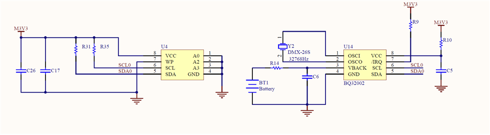
Hardware schematic for BQ32002 is as follows:

Please tell me how to solve it and what changes I would make.

Thanks in advance.
Banbom

  • Hi,

    On the hardware side, is there pull up resistors on the SDA and SCL line. I could not see it in those pictures. 

    About the software, do you mean your receive message from BQ32002 is not correct? Have you use a logic analyzer to capture the signal on the I2C bus and check if it is correct on the bus?

    Best regards,

    Cash Hao 

  • Hi Cash,

    Thanks for your reply. More infos, There're two I2C devices on this same I2C bus, where you can find the previous I2C device has also pull up resistors as follows:

    the previous I2C device can be operated normally, and I2c operation read/write on this device is okay.  The problem is the I2C read/write on BQ32002, I couldn't identify these receive message from BQ32002 is right or not, it seems the value(times, such as seconds/minutes/hours/month/yeah) hasn't been set to BQ32002 the correct value as the code.

    Regards,
    Banbom.

  • The most striking thing about the read-back data is that each should be (at least in the low-order digit) BCD, and only 3 of the 7 are. The data sheet claims that, even supposing it were written wrong, invalid data will be repaired (it doesn't say how exactly) over time.

    A couple of quick experiments:

    1) Before you do any of the fixups, just read all 10 registers and see if they look anything like the datasheet says.

    2) Extend your loop delay from 0.25 sec -> 1 second; during this time the SECONDS register should have been "repaired" (somehow).

    What is the other device on the bus? It reminds one of an EEPROM/FRAM; those are usually address 0x5X rather than 0x6X, but I'm trying not to assume anything.

  • Hi Bruce,

    Thanks for your quick reply.  Based on your suggestion,  a slight code change as your mentioned BCD translation.
    As follows:

    //******************************************************************************
    //   MSP430F552x Demo - USCI_B0, I2C Master multiple byte TX/RX
    //
    //   Description: I2C master communicates to I2C slave sending and receiving
    //   3 different messages of different length. I2C master will enter LPM0 mode
    //   while waiting for the messages to be sent/receiving using I2C interrupt.
    //   ACLK = NA, MCLK = SMCLK = DCO 16MHz.
    //
    //                                     /|\ /|\
    //                   MSP430F5529       4.7k |
    //                 -----------------    |  4.7k
    //            /|\ |             P3.1|---+---|-- I2C Clock (UCB0SCL)
    //             |  |                 |       |
    //             ---|RST          P3.0|-------+-- I2C Data (UCB0SDA)
    //                |                 |
    //                |                 |
    //                |                 |
    //                |                 |
    //                |                 |
    //                |                 |
    //
    //   Nima Eskandari
    //   Texas Instruments Inc.
    //   April 2017
    //   Built with CCS V7.0
    //******************************************************************************
    
    #include <msp430.h> 
    #include <stdint.h>
    #include <stdbool.h>
    #include <string.h>
    
    //******************************************************************************
    // Example Commands ************************************************************
    //******************************************************************************
    
    //#define SLAVE_ADDR  0x48
    #define SLAVE_ADDR 0x68
    
    /* CMD_TYPE_X_SLAVE are example commands the master sends to the slave.
     * The slave will send example SlaveTypeX buffers in response.
     *
     * CMD_TYPE_X_MASTER are example commands the master sends to the slave.
     * The slave will initialize itself to receive MasterTypeX example buffers.
     * */
    
    #define CMD_TYPE_0_SLAVE      0
    #define CMD_TYPE_1_SLAVE      1
    #define CMD_TYPE_2_SLAVE      2
    
    #define CMD_TYPE_0_MASTER      0
    #define CMD_TYPE_1_MASTER      4
    #define CMD_TYPE_2_MASTER      5
    
    #define TYPE_0_LENGTH   7
    #define TYPE_1_LENGTH   2
    #define TYPE_2_LENGTH   6
    
    #define MAX_BUFFER_SIZE     20
    
    /* MasterTypeX are example buffers initialized in the master, they will be
     * sent by the master to the slave.
     * SlaveTypeX are example buffers initialized in the slave, they will be
     * sent by the slave to the master.
     * */
    
    uint8_t MasterType2 [TYPE_2_LENGTH] = {'F', '4', '1', '9', '2', 'B'};
    uint8_t MasterType1 [TYPE_1_LENGTH] = { 8, 9};
    uint8_t MasterType0 [TYPE_0_LENGTH] = { 85, 88, 35, 1, 49, 18, 35}; // {28/04/2023 01:57:01 pm}
    
    
    uint8_t SlaveType2 [TYPE_2_LENGTH] = {0};
    uint8_t SlaveType1 [TYPE_1_LENGTH] = {0};
    uint8_t SlaveType0 [TYPE_0_LENGTH] = {0};
    uint8_t SlaveByte [1] = {0};
    
    
    //******************************************************************************
    // General I2C State Machine ***************************************************
    //******************************************************************************
    
    typedef enum I2C_ModeEnum{
        IDLE_MODE,
        NACK_MODE,
        TX_REG_ADDRESS_MODE,
        RX_REG_ADDRESS_MODE,
        TX_DATA_MODE,
        RX_DATA_MODE,
        SWITCH_TO_RX_MODE,
        SWITHC_TO_TX_MODE,
        TIMEOUT_MODE
    } I2C_Mode;
    
    /* Used to track the state of the software state machine*/
    I2C_Mode MasterMode = IDLE_MODE;
    
    /* The Register Address/Command to use*/
    uint8_t TransmitRegAddr = 0;
    
    /* ReceiveBuffer: Buffer used to receive data in the ISR
     * RXByteCtr: Number of bytes left to receive
     * ReceiveIndex: The index of the next byte to be received in ReceiveBuffer
     * TransmitBuffer: Buffer used to transmit data in the ISR
     * TXByteCtr: Number of bytes left to transfer
     * TransmitIndex: The index of the next byte to be transmitted in TransmitBuffer
     * */
    uint8_t ReceiveBuffer[MAX_BUFFER_SIZE] = {0};
    uint8_t RXByteCtr = 0;
    uint8_t ReceiveIndex = 0;
    uint8_t TransmitBuffer[MAX_BUFFER_SIZE] = {0};
    uint8_t TXByteCtr = 0;
    uint8_t TransmitIndex = 0;
    
    /* I2C Write and Read Functions */
    
    /* For slave device with dev_addr, writes the data specified in *reg_data
     *
     * dev_addr: The slave device address.
     *           Example: SLAVE_ADDR
     * reg_addr: The register or command to send to the slave.
     *           Example: CMD_TYPE_0_MASTER
     * *reg_data: The buffer to write
     *           Example: MasterType0
     * count: The length of *reg_data
     *           Example: TYPE_0_LENGTH
     *  */
    I2C_Mode I2C_Master_WriteReg(uint8_t dev_addr, uint8_t reg_addr, uint8_t *reg_data, uint8_t count);
    
    /* For slave device with dev_addr, read the data specified in slaves reg_addr.
     * The received data is available in ReceiveBuffer
     *
     * dev_addr: The slave device address.
     *           Example: SLAVE_ADDR
     * reg_addr: The register or command to send to the slave.
     *           Example: CMD_TYPE_0_SLAVE
     * count: The length of data to read
     *           Example: TYPE_0_LENGTH
     *  */
    I2C_Mode I2C_Master_ReadReg(uint8_t dev_addr, uint8_t reg_addr, uint8_t count);
    void CopyArray(uint8_t *source, uint8_t *dest, uint8_t count);
    
    I2C_Mode I2C_Master_ReadReg(uint8_t dev_addr, uint8_t reg_addr, uint8_t count)
    {
        /* Initialize state machine */
        MasterMode = TX_REG_ADDRESS_MODE;
        TransmitRegAddr = reg_addr;
        RXByteCtr = count;
        TXByteCtr = 0;
        ReceiveIndex = 0;
        TransmitIndex = 0;
    
        /* Initialize slave address and interrupts */
        UCB0I2CSA = dev_addr;
        UCB0IFG &= ~(UCTXIFG + UCRXIFG);       // Clear any pending interrupts
        UCB0IE &= ~UCRXIE;                       // Disable RX interrupt
        UCB0IE |= UCTXIE;                        // Enable TX interrupt
    
        UCB0CTL1 |= UCTR + UCTXSTT;             // I2C TX, start condition
        __bis_SR_register(LPM0_bits + GIE);              // Enter LPM0 w/ interrupts
    
        return MasterMode;
    
    }
    
    
    I2C_Mode I2C_Master_WriteReg(uint8_t dev_addr, uint8_t reg_addr, uint8_t *reg_data, uint8_t count)
    {
        /* Initialize state machine */
        MasterMode = TX_REG_ADDRESS_MODE;
        TransmitRegAddr = reg_addr;
    
        //Copy register data to TransmitBuffer
        CopyArray(reg_data, TransmitBuffer, count);
    
        TXByteCtr = count;
        RXByteCtr = 0;
        ReceiveIndex = 0;
        TransmitIndex = 0;
    
        /* Initialize slave address and interrupts */
        UCB0I2CSA = dev_addr;
        UCB0IFG &= ~(UCTXIFG + UCRXIFG);       // Clear any pending interrupts
        UCB0IE &= ~UCRXIE;                       // Disable RX interrupt
        UCB0IE |= UCTXIE;                        // Enable TX interrupt
    
        UCB0CTL1 |= UCTR + UCTXSTT;             // I2C TX, start condition
        __bis_SR_register(LPM0_bits + GIE);              // Enter LPM0 w/ interrupts
    
        return MasterMode;
    }
    
    void CopyArray(uint8_t *source, uint8_t *dest, uint8_t count)
    {
        uint8_t copyIndex = 0;
        for (copyIndex = 0; copyIndex < count; copyIndex++)
        {
            dest[copyIndex] = source[copyIndex];
        }
    }
    
    //******************************************************************************
    // Device Initialization *******************************************************
    //******************************************************************************
    
    void initClockTo16MHz()
    {
        UCSCTL3 |= SELREF_2;                      // Set DCO FLL reference = REFO
        UCSCTL4 |= SELA_2;                        // Set ACLK = REFO
        __bis_SR_register(SCG0);                  // Disable the FLL control loop
        UCSCTL0 = 0x0000;                         // Set lowest possible DCOx, MODx
        UCSCTL1 = DCORSEL_5;                      // Select DCO range 16MHz operation
        UCSCTL2 = FLLD_0 + 487;                   // Set DCO Multiplier for 16MHz
                                                  // (N + 1) * FLLRef = Fdco
                                                  // (487 + 1) * 32768 = 16MHz
                                                  // Set FLL Div = fDCOCLK
        __bic_SR_register(SCG0);                  // Enable the FLL control loop
    
        // Worst-case settling time for the DCO when the DCO range bits have been
        // changed is n x 32 x 32 x f_MCLK / f_FLL_reference. See UCS chapter in 5xx
        // UG for optimization.
        // 32 x 32 x 16 MHz / 32,768 Hz = 500000 = MCLK cycles for DCO to settle
        __delay_cycles(500000);//
        // Loop until XT1,XT2 & DCO fault flag is cleared
        do
        {
            UCSCTL7 &= ~(XT2OFFG + XT1LFOFFG + DCOFFG); // Clear XT2,XT1,DCO fault flags
            SFRIFG1 &= ~OFIFG;                          // Clear fault flags
        }while (SFRIFG1&OFIFG);                         // Test oscillator fault flag
    }
    
    uint16_t setVCoreUp(uint8_t level){
        uint32_t PMMRIE_backup, SVSMHCTL_backup, SVSMLCTL_backup;
    
        //The code flow for increasing the Vcore has been altered to work around
        //the erratum FLASH37.
        //Please refer to the Errata sheet to know if a specific device is affected
        //DO NOT ALTER THIS FUNCTION
    
        //Open PMM registers for write access
        PMMCTL0_H = 0xA5;
    
        //Disable dedicated Interrupts
        //Backup all registers
        PMMRIE_backup = PMMRIE;
        PMMRIE &= ~(SVMHVLRPE | SVSHPE | SVMLVLRPE |
                    SVSLPE | SVMHVLRIE | SVMHIE |
                    SVSMHDLYIE | SVMLVLRIE | SVMLIE |
                    SVSMLDLYIE
                    );
        SVSMHCTL_backup = SVSMHCTL;
        SVSMLCTL_backup = SVSMLCTL;
    
        //Clear flags
        PMMIFG = 0;
    
        //Set SVM highside to new level and check if a VCore increase is possible
        SVSMHCTL = SVMHE | SVSHE | (SVSMHRRL0 * level);
    
        //Wait until SVM highside is settled
        while((PMMIFG & SVSMHDLYIFG) == 0)
        {
            ;
        }
    
        //Clear flag
        PMMIFG &= ~SVSMHDLYIFG;
    
        //Check if a VCore increase is possible
        if((PMMIFG & SVMHIFG) == SVMHIFG)
        {
            //-> Vcc is too low for a Vcore increase
            //recover the previous settings
            PMMIFG &= ~SVSMHDLYIFG;
            SVSMHCTL = SVSMHCTL_backup;
    
            //Wait until SVM highside is settled
            while((PMMIFG & SVSMHDLYIFG) == 0)
            {
                ;
            }
    
            //Clear all Flags
            PMMIFG &= ~(SVMHVLRIFG | SVMHIFG | SVSMHDLYIFG |
                         SVMLVLRIFG | SVMLIFG |
                         SVSMLDLYIFG
                         );
    
            //Restore PMM interrupt enable register
            PMMRIE = PMMRIE_backup;
            //Lock PMM registers for write access
            PMMCTL0_H = 0x00;
            //return: voltage not set
            return false;
        }
    
        //Set also SVS highside to new level
        //Vcc is high enough for a Vcore increase
        SVSMHCTL |= (SVSHRVL0 * level);
    
        //Wait until SVM highside is settled
        while((PMMIFG & SVSMHDLYIFG) == 0)
        {
            ;
        }
    
        //Clear flag
        PMMIFG &= ~SVSMHDLYIFG;
    
        //Set VCore to new level
        PMMCTL0_L = PMMCOREV0 * level;
    
        //Set SVM, SVS low side to new level
        SVSMLCTL = SVMLE | (SVSMLRRL0 * level) |
                   SVSLE | (SVSLRVL0 * level);
    
        //Wait until SVM, SVS low side is settled
        while((PMMIFG & SVSMLDLYIFG) == 0)
        {
            ;
        }
    
        //Clear flag
        PMMIFG &= ~SVSMLDLYIFG;
        //SVS, SVM core and high side are now set to protect for the new core level
    
        //Restore Low side settings
        //Clear all other bits _except_ level settings
        SVSMLCTL &= (SVSLRVL0 + SVSLRVL1 + SVSMLRRL0 +
                     SVSMLRRL1 + SVSMLRRL2
                     );
    
        //Clear level settings in the backup register,keep all other bits
        SVSMLCTL_backup &=
            ~(SVSLRVL0 + SVSLRVL1 + SVSMLRRL0 + SVSMLRRL1 + SVSMLRRL2);
    
        //Restore low-side SVS monitor settings
        SVSMLCTL |= SVSMLCTL_backup;
    
        //Restore High side settings
        //Clear all other bits except level settings
        SVSMHCTL &= (SVSHRVL0 + SVSHRVL1 +
                     SVSMHRRL0 + SVSMHRRL1 +
                     SVSMHRRL2
                     );
    
        //Clear level settings in the backup register,keep all other bits
        SVSMHCTL_backup &=
            ~(SVSHRVL0 + SVSHRVL1 + SVSMHRRL0 + SVSMHRRL1 + SVSMHRRL2);
    
        //Restore backup
        SVSMHCTL |= SVSMHCTL_backup;
    
        //Wait until high side, low side settled
        while(((PMMIFG & SVSMLDLYIFG) == 0) &&
              ((PMMIFG & SVSMHDLYIFG) == 0))
        {
            ;
        }
    
        //Clear all Flags
        PMMIFG &= ~(SVMHVLRIFG | SVMHIFG | SVSMHDLYIFG |
                    SVMLVLRIFG | SVMLIFG | SVSMLDLYIFG
                    );
    
        //Restore PMM interrupt enable register
        PMMRIE = PMMRIE_backup;
    
        //Lock PMM registers for write access
        PMMCTL0_H = 0x00;
    
        return true;
    }
    
    bool increaseVCoreToLevel2()
    {
        uint8_t level = 2;
        uint8_t actlevel;
        bool status = true;
    
        //Set Mask for Max. level
        level &= PMMCOREV_3;
    
        //Get actual VCore
        actlevel = PMMCTL0 & PMMCOREV_3;
    
        //step by step increase or decrease
        while((level != actlevel) && (status == true))
        {
            if(level > actlevel)
            {
                status = setVCoreUp(++actlevel);
            }
        }
    
        return (status);
    }
    
    void initGPIO()
    {
        //LEDs
        P1OUT = 0x00;                             // P1 setup for LED & reset output
        P1DIR |= BIT0;
    
        P4DIR |= BIT7;
        P4OUT &= ~(BIT7);
    
        //I2C Pins
        P3SEL |= BIT0 + BIT1;                     // P3.0,1 option select
    
        P2OUT=0X00; 
        P2DIR=0XFF; 
    
        //#define Buzzer_OFF      
        P2OUT&=~0X80;
    }
    
    void initI2C()
    {
        UCB0CTL1 |= UCSWRST;                      // Enable SW reset
        UCB0CTL0 = UCMST + UCMODE_3 + UCSYNC;     // I2C Master, synchronous mode
        UCB0CTL1 = UCSSEL_2 + UCSWRST;            // Use SMCLK, keep SW reset
        UCB0BR0 = 160;                            // fSCL = SMCLK/160 = ~100kHz
        UCB0BR1 = 0;
        UCB0I2CSA = SLAVE_ADDR;                   // Slave Address is 048h
        UCB0CTL1 &= ~UCSWRST;                     // Clear SW reset, resume operation
        UCB0IE |= UCNACKIE;
    }
    
    //******************************************************************************
    // Main ************************************************************************
    // Send and receive three messages containing the example commands *************
    //******************************************************************************
    #define BQ32K_SECONDS		0x00	/* Seconds register address */
    #define BQ32K_SECONDS_MASK	0x7F	/* Mask over seconds value */
    #define BQ32K_STOP		0x80	/* Oscillator Stop flat */
    
    #define BQ32K_MINUTES		0x01	/* Minutes register address */
    #define BQ32K_MINUTES_MASK	0x7F	/* Mask over minutes value */
    #define BQ32K_OF		0x80	/* Oscillator Failure flag */
    
    #define BQ32K_HOURS_MASK	0x3F	/* Mask over hours value */
    #define BQ32K_CENT		0x40	/* Century flag */
    #define BQ32K_CENT_EN		0x80	/* Century flag enable bit */
    
    #define BQ32K_CALIBRATION	0x07	/* CAL_CFG1, calibration and control */
    #define BQ32K_TCH2		0x08	/* Trickle charge enable */
    #define BQ32K_CFG2		0x09	/* Trickle charger control */
    
    #define bcd2bin(x)    (((x) & 0x0f) + ((x) >> 4) * 10)
    #define bin2bcd(x)    ((((x) / 10) << 4) + (x) % 10)
    
    struct BQ32K_REGS {
    	uint8_t		seconds;
    	uint8_t		minutes;
    	uint8_t		cent_hours;
    	uint8_t		day;
    	uint8_t		date;
    	uint8_t		month;
    	uint8_t		years;
    };
    
    struct SysRtcTime {
    	uint8_t tm_sec;
    	uint8_t tm_min;
    	uint8_t tm_hour;
    	uint8_t tm_mday;
    	uint8_t tm_mon;
    	uint8_t tm_year;
    	uint8_t tm_wday;
    	uint8_t tm_yday;
    	uint8_t tm_isdst;
    };
    
    uint8_t BQ32KRtcRead(struct SysRtcTime *tm)
    {
    	struct BQ32K_REGS regs;
    	uint8_t error;
    
    	error = I2C_Master_ReadReg(SLAVE_ADDR,  0, sizeof(regs));
            CopyArray(ReceiveBuffer, (uint8_t *)&regs, sizeof(regs));
    	if (error != IDLE_MODE)
    		return 0x1;
    
    	/*
    	 * In case of oscillator failure, the register contents should be
    	 * considered invalid. The flag is cleared the next time the RTC is set.
    	 */
    	if (regs.minutes & BQ32K_OF)
    		return 0x1;
    
    	tm->tm_sec = bcd2bin(regs.seconds & BQ32K_SECONDS_MASK);
    	tm->tm_min = bcd2bin(regs.minutes & BQ32K_MINUTES_MASK);
    	tm->tm_hour = bcd2bin(regs.cent_hours & BQ32K_HOURS_MASK);
    	tm->tm_mday = bcd2bin(regs.date);
    	tm->tm_wday = bcd2bin(regs.day) - 1;
    	tm->tm_mon = bcd2bin(regs.month) - 1;
    	tm->tm_year = bcd2bin(regs.years) +
    				((regs.cent_hours & BQ32K_CENT) ? 100 : 0);
    
    	return 0;
    }
    
    uint8_t BQ32KRtcSet(struct SysRtcTime *tm)
    {
    	struct BQ32K_REGS regs;
    
    	regs.seconds = bin2bcd(tm->tm_sec);
    	regs.minutes = bin2bcd(tm->tm_min);
    	regs.cent_hours = bin2bcd(tm->tm_hour) | BQ32K_CENT_EN;
    	regs.day = bin2bcd(tm->tm_wday + 1);
    	regs.date = bin2bcd(tm->tm_mday);
    	regs.month = bin2bcd(tm->tm_mon + 1);
    
    	if (tm->tm_year >= 100) {
    		regs.cent_hours |= BQ32K_CENT;
    		regs.years = bin2bcd(tm->tm_year - 100);
    	} else
    		regs.years = bin2bcd(tm->tm_year);
    
            I2C_Master_WriteReg(SLAVE_ADDR, CMD_TYPE_0_MASTER, (uint8_t *)&regs, sizeof(regs));
            
            return 0;
    }
    
    int main(void) {
        struct SysRtcTime Systm;
     
        WDTCTL = WDTPW | WDTHOLD;                 // Stop watchdog timer
    
        increaseVCoreToLevel2();
        initClockTo16MHz();
        initGPIO();
        initI2C();
    
        {
            //int error;
            uint8_t reg;
            
            /* Check Oscillator Stop flag */
            I2C_Master_ReadReg(SLAVE_ADDR, BQ32K_SECONDS, 1);
            CopyArray(ReceiveBuffer, SlaveByte, 1);
            reg=SlaveByte[0];
        
            if (reg & BQ32K_STOP) {
                // Oscillator was halted. Restarting
                reg &= ~BQ32K_STOP;
                SlaveByte[0]=reg;
                I2C_Master_WriteReg(SLAVE_ADDR, BQ32K_SECONDS, SlaveByte, 1);
            }
        
            /* Check Oscillator Failure flag */
            I2C_Master_ReadReg(SLAVE_ADDR, BQ32K_MINUTES, 1);
            CopyArray(ReceiveBuffer, SlaveByte, 1);
            reg=SlaveByte[0];
            if (reg & BQ32K_OF)
            {
                //Oscillator Failure. Check RTC battery
                reg &= ~BQ32K_OF;
                SlaveByte[0]=reg;
                I2C_Master_WriteReg(SLAVE_ADDR, BQ32K_MINUTES, SlaveByte, 1);
            }
    
        }
    
            __delay_cycles(4000000);
            __delay_cycles(4000000);
            __delay_cycles(4000000);
            __delay_cycles(4000000);
        
        memset((void *)&Systm, 0, sizeof(Systm));
        
        Systm.tm_year=124;  /* 2024/08/07/08:52:12 */
        Systm.tm_mon=8;
        Systm.tm_mday=7;
        Systm.tm_wday=3;
        Systm.tm_hour=8;
        Systm.tm_min=52;
        Systm.tm_sec=12;
    
        BQ32KRtcSet(&Systm);        
        
        while(1)
        {
            __delay_cycles(4000000);
            __delay_cycles(4000000);
            __delay_cycles(4000000);
            __delay_cycles(4000000);
            
            memset((void *)&Systm, 0, sizeof(Systm));
            BQ32KRtcRead(&Systm);
        }
    
        __bis_SR_register(LPM0_bits + GIE);
        return 0;
    }
    
    //******************************************************************************
    // I2C Interrupt ***************************************************************
    //******************************************************************************
    
    #if defined(__TI_COMPILER_VERSION__) || defined(__IAR_SYSTEMS_ICC__)
    #pragma vector=USCI_B0_VECTOR
    __interrupt void USCI_B0_ISR(void)
    #elif defined(__GNUC__)
    void __attribute__ ((interrupt(USCI_B0_VECTOR))) USCI_B0_ISR (void)
    #else
    #error Compiler not supported!
    #endif
    {
      //Must read from UCB0RXBUF
      uint8_t rx_val = 0;
    
      switch(__even_in_range(UCB0IV,0xC))
      {
        case USCI_NONE:break;                             // Vector 0 - no interrupt
        case USCI_I2C_UCALIFG:break;                      // Interrupt Vector: I2C Mode: UCALIFG
        case USCI_I2C_UCNACKIFG:break;                    // Interrupt Vector: I2C Mode: UCNACKIFG
        case USCI_I2C_UCSTTIFG:break;                     // Interrupt Vector: I2C Mode: UCSTTIFG
        case USCI_I2C_UCSTPIFG:break;                     // Interrupt Vector: I2C Mode: UCSTPIFG
        case USCI_I2C_UCRXIFG:
            rx_val = UCB0RXBUF;
            if (RXByteCtr)
            {
              ReceiveBuffer[ReceiveIndex++] = rx_val;
              RXByteCtr--;
            }
    
            if (RXByteCtr == 1)
            {
              UCB0CTL1 |= UCTXSTP;
            }
            else if (RXByteCtr == 0)
            {
              UCB0IE &= ~UCRXIE;
              MasterMode = IDLE_MODE;
              __bic_SR_register_on_exit(CPUOFF);      // Exit LPM0
            }
            break;                      // Interrupt Vector: I2C Mode: UCRXIFG
        case USCI_I2C_UCTXIFG:
            switch (MasterMode)
            {
              case TX_REG_ADDRESS_MODE:
                  UCB0TXBUF = TransmitRegAddr;
                  if (RXByteCtr)
                      MasterMode = SWITCH_TO_RX_MODE;   // Need to start receiving now
                  else
                      MasterMode = TX_DATA_MODE;        // Continue to transmission with the data in Transmit Buffer
                  break;
    
              case SWITCH_TO_RX_MODE:
                  UCB0IE |= UCRXIE;              // Enable RX interrupt
                  UCB0IE &= ~UCTXIE;             // Disable TX interrupt
                  UCB0CTL1 &= ~UCTR;            // Switch to receiver
                  MasterMode = RX_DATA_MODE;    // State state is to receive data
                  UCB0CTL1 |= UCTXSTT;          // Send repeated start
                  if (RXByteCtr == 1)
                  {
                      //Must send stop since this is the N-1 byte
                      while((UCB0CTL1 & UCTXSTT));
                      UCB0CTL1 |= UCTXSTP;      // Send stop condition
                  }
                  break;
    
              case TX_DATA_MODE:
                  if (TXByteCtr)
                  {
                      UCB0TXBUF = TransmitBuffer[TransmitIndex++];
                      TXByteCtr--;
                  }
                  else
                  {
                      //Done with transmission
                      UCB0CTL1 |= UCTXSTP;     // Send stop condition
                      MasterMode = IDLE_MODE;
                      UCB0IE &= ~UCTXIE;                       // disable TX interrupt
                      __bic_SR_register_on_exit(CPUOFF);      // Exit LPM0
                  }
                  break;
    
              default:
                  __no_operation();
                  break;
            }
            break;                      // Interrupt Vector: I2C Mode: UCTXIFG
        default: break;
      }
    }


    Still it read and got the wrong data each loop ( about 1s) as follows during 'step debug' by USB JTAG.

    The other device is one EEPROM, which i2c devices address is 0xA0(shit one bit, it's 0x50). current test code is only for BQ32002 rtc read/write test.
    I have another test code for such EEPROM device read/write test, which can do the right R/W operation.

    Regards,
    Banbom

  • Hi Banbom,

    Do you have a logic analyzer to capture the data on the I2C bus? Can you compare it with the readings in the MCU and check if they match each other?

    Best regards,

    Cash Hao

  • This data is not just invalid, it's identical to what you were getting yesterday, as though the device isn't running at all. Do you have a way of telling whether the crystal is oscillating? (Probing with a scope is hit-and-miss, but it sometimes works.)

    Also, what's the purpose of R10? I don't see it in the suggested circuit in data sheet (SLUSA96B) Fig 8.

  • Hi Cash,

    Yes, I want to. but I have no logic analyzer now. Besides using logic analyzer, from current code, could you please give some advice? Thanks.

  • Hi,

    On the software side, I agree with Bruce's comment. I do not see obvious error in the code. 

    Best regards,

    Cash Hao

  • I don't have your equipment, but I just tried this code (with some insubstantial adjustments) using an F5529 and an LIS3DH, and I was able to read its registers. I think this code is doing what we expect.

    What is the purpose of R10? Do you see 3.3V at the BQ32002 VCC pin (or at least >2.4V)?

    [Edit: Fixed typo]

  • Hi Bruce,

    Thanks for your found. R10 is one current limiting resistor,after i removed it. Now I got the correct value as follows.
    However, after each 1s delay loop, the second register of BQ32002 is still the same value 12, not any change or move forward.

    Regards,
    Banbom.

  • First guess is that the oscillator isn't running. They don't recommend a load capacitance for the crystal, but your 12.5pF is pretty typical.

    Datasheet Sec 7.6.2 (SECONDS), under the STOP bit, suggests that "STOP can be written to 1 and then written to 0 to force start the oscillator.". It may be worth trying that.

**Attention** This is a public forum